Running a physical model on a Speedgoat.
 Speedgoat
I have said in some posts that you can do everything with an FPGA, and although that affirmation is false, an FPGA cannot do an omelet for example, you can indeed do many things with an FPGA. Because of their parallel nature, and speed, FPGA are widely used to implement complex control algorithms to control complex systems, but the system is what it is. It can be an AC motor, a wind turbine, a pneumatic cylinder, or a power supply but … what do you think if I said that all those systems can also be inside of an FPGA? let’s think… All the systems, either mechanical, electrical or pneumatical can be modelized as a set of mathematical equations which we call model. The complexity of the system will also determine the complexity of the model, so very simple systems like an RC filter can be modelized using a few equations, and other models used to model the efforts of a bridge will have more than a few equations, but mathematical equations at the end. FPGAs, are very good at calculating mathematical operations, so, can we implement on an FPGA the mathematical model of a physical system? the answer is yes, and we are going to do it using Speedgoat and Simulink Real-Time (a MATLAB toolbox).
As we saw in this post, Speedgoat is a company that builds real-time target computers with a CPU and one or more FPGAs inside. The FPGA is connected to ADCs, DACs and digital IOs, so it is easy to implement the mathematical model of a physical system on the FPGA, and use the DAC to extract the signals of the model. At this point we know where the model will be, but, how about the equations? Generating the mathematical model of simple models is easy, but for complex models, it has difficult, so we need a tool that generates the mathematical model of a given physical model. For that task, MATLAB is the best option.
So, we have MATLAB to generate the model and the Speedgoat Baseline where we will deploy the model. To show the flow of generating and deploying a model, we are going to use a Buck power supply.
First of all, we need to install the packages needed for HDL Coder. It is essentially a Board support package for the Speedgoat Baseline, as we did with the Picozed FMC board. To install this package we need to download it from the Speedgoat customer portal, end execute the installer script.
>> hdlCoder_integration_package_installer
HDL coder integration package available for your MATLAB release R2022b:
 => Do you want to install the HDL coder integration package(s)? [y]/n: y
 - Closing all open models before proceeding: OK
 - Installing: R2022b_IO397_50k_HCIP_v2.0: OK
 - Rehashing toolbox: OK
---
Note: There is a known issue with Xilinx Vivado 2020.2 when using Aurora 64B66B IP core.
Please consult our release notes for more details on required patches to install.
---
HDL Coder Integration Package installed.
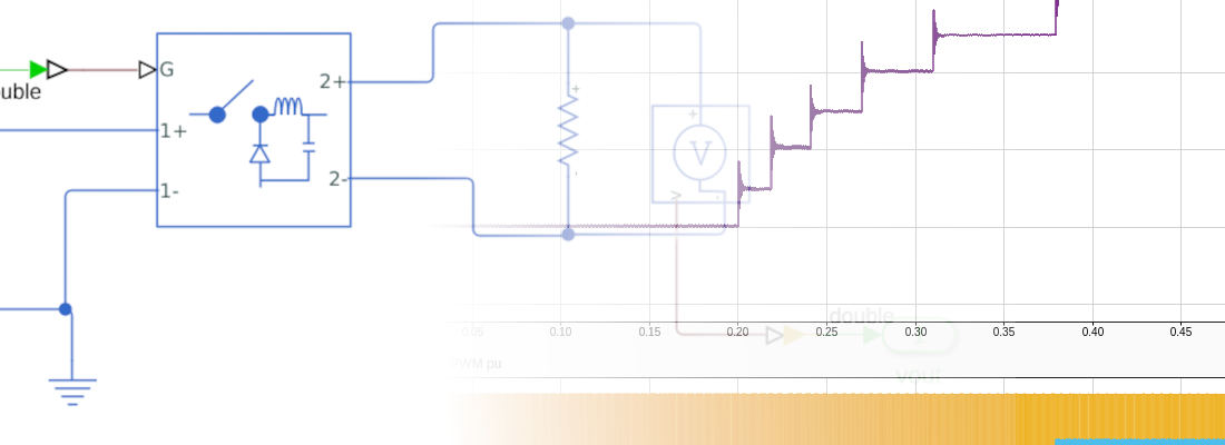
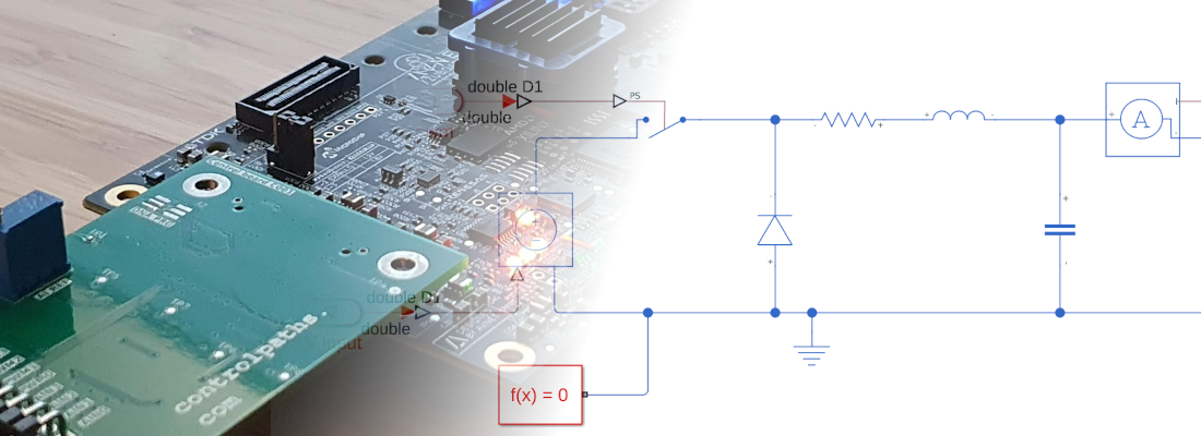
The model we are going to simulate is an asynchronous Buck power supply. This power supply only has one controlled switching element. Since we are going to control the output voltage, we need to add a voltage meter in the output and a current meter. All the elements needed to create the model are available in the Simscape Electrical Library. Once all the elements are connected, the resulting diagram will be like the shown below.

This will be the electrical model that we are going to simulate with the Speedgoat. This model has one input to control the switching element, and two double outputs for the current and the voltage. It is important when we are working with Simscape models to add to the model the corresponding elements to transform the signals from a Simulink model to a Simscape model, as well as add a reference point for the solver.
Once our electrical model is complete, we can move the model into a subsystem. Then, on the top model, we are going to add the blocks needed to adapt the signals to the Speedgoat inputs and outputs.
Since all the signals inside the Simscape model are double, we are going to add three Signal Specification blocks from the Simulink library configured as double. Then, the PWM input, connected to the switching element, will be connected to a boolean signal, since the PWM will be connected to a digital input, so we need to add a Convert block in the middle of the line. Regarding the analog outputs, we will need to add a gain to convert from the units of the model to a the voltage output of the Speedgoat. Also, we will add a Convert block to convert the double signal into a 16 bit integer as defined in the documentation.

In order to configure the gain for the analog channels, we need to know the features of the IO397’s analog outputs. In this case, the IO397 has 4 analog outputs with a resolution of 16 bits and an output range is +-10 volts. For this article, I going to connect the analog output to a 12 bits ADC with an input range from 0 to 3 volts, so I want that the maximum output that I expect fits in that range. The resistor is calculated for a maximum current of 10 Amps, so the gain for the current analog output will be:
\[A_I = \frac{3}{10} \cdot \frac{2^{15}}{10}\]For the output voltage analog output, the input voltage is 15 volts, so this is the maximum voltage of the output as well. The gain, in this case, will be:
\[A_V = \frac{3}{15} \cdot \frac{2^{15}}{10}\]An extra output has to be added to be used as DAC clock enable or trigger. This output is connected to a constant value of ‘1’ to trigger the DACs at the maximum rate.

At this point, we have the model that will run on the FPGA complete. All the elements of this model will be inside a subsystem named FPGA. The name of the subsystem will not define that this subsystem will run into the FPGA, but it is useful for better understanding.
In order to simulate the model to verify that all is correct, we can add some external stimulus for the inputs, in this case, I have added a PWM generator with a variable duty cycle, and two gains for the output to convert the output signals again to its original range.

Finally, to execute the simulation, we need to define a sampling time. This variable is used on the first block, and then the sampling time will be propagated.
Ts = 1e-6;
Now, clicking over the RUN button, the simulation will be executed for the configured time.

Now we are going to begin the transformation of the model in a mathematical model to be implemented on the FPGA. First, we need to know that not the entire blocks in the Simulink library are compatible with HDL code generation. We can generate the HDL code of a Delay block, or a multiplication, however, other blocks like the electrical elements from Simscape library are not immediately compatible with HDL Coder. For these blocks, MATLAB can transform those electrical blocks into an HDL coder compatible model. To do this, MATLAB uses the mathematical model of the electrical elements, and generates automatically a space-state representation of the entire circuit. Then, is this space-state model which is used to generate the RTL code. To create this electrical model, we need to use a local solver for the Simscape electrical network. Then, we are going to launch the Simscape HDL Workflow Advisor using the command sschdladvisor. We need to create the space-state model just for the Simscape circuit, so we need to navigate into that subsystem.
set_param('hdl_buck/FPGA/Buck/Solver Configuration','DoFixedCost','on')
set_param('hdl_buck/FPGA/Buck/Solver Configuration','MaxNonlinIter','2')

sschdladvisor('hdl_buck')
The window of the Simscape HDL Workflow Advisor is pretty similar to the window of the HDL Workflow Advisor with different steps that must be executed. To execute all the steps, we can click on Run All. The step where Simulink extracts all the nodes of the circuit, and generate the equations for each one, the one named Extract Equations, can take some minutes according to the complexity of your electrical circuit and the total simulation time set in the source model, so you may have to be patient.

Once the generation is finished, the folder /sschld will be created in your project. If we navigate inside this folder, we will see that a new Simulink model has been created with the name gmStateSpaceHDL_hdl_buck. That model is similar to the original one on the top level, but if we navigate inside the subsystem we will see that the electrical circuit has been replaced by a set of mathematical expressions, and a space-state block. The key of this model is that, even though the model is different than the original one, its behavior is the same.

If we navigate inside the red block we can see the mathematical model that Simulink has generated, built just with Simulink blocks.

We can check the model executing the same simulation we executed before, and the response will be the same as the one obtained with the electrical model.

Although this step could seem simple since we only have to press a button, this step is the most important in this flow, because the transformation of the electrical model into a mathematical model is what will determine later the confidence of our simulation. In other words, this step is responsible for making the model look like the real circuit.
Once we have the electrical model translated into a mathematical model that HDL Coder can translate into an RTL code, the next is to generate the RTL code of all the elements that will run into the FPGA. To do that, we will use the HDL Workflow Advisor, but before, we need to make some changes in the model. First, we need to modify the resolution of double signals into single signals for an optimized FPGA representation of floating-point signals. To do that the Signal Specification blocks we added before are very useful. Also, we are going to execute the command hdlsetup which will modify some settings of the model, and finally we can execute the command hdladvisor.
hdlsetuptoolpath('ToolName','Xilinx Vivado','ToolPath','/media/pablo/data_m2/xilinx/Vivado/2022.2/bin/vivado');

set_param('gmStateSpaceHDL_HIL_buck', 'SimulationCommand', 'Update')

set_param('gmStateSpaceHDL_HIL_buck/FPGA/Signal Specification','OutDataTypeStr','single');
set_param('gmStateSpaceHDL_HIL_buck/FPGA/Signal Specification1','OutDataTypeStr','single');
set_param('gmStateSpaceHDL_HIL_buck/FPGA/Signal Specification2','OutDataTypeStr','single');

hdlsetup('gmStateSpaceHDL_HIL_buck')

hdladvisor('gmStateSpaceHDL_HIL_buck/FPGA')
The next steps are familiar to us since are the same as we execute in this post, but changing the target. In this occasion, we are going to use the workflow Simulink Real-Time FPGA I/O, and the target Speedgoat IO397-50k. As a too, Vivado will be selected automatically when Speedgoat target platform is chosen, and finally, the FPGA will be also selected automatically.

In the next step, all the settings are already selected since they are related to the hardware interfaces.

Now, we have to select where the model signals will be connected in the Speedgoat. For this model we have the PWM input, two analog outputs for the output voltage and the output current, and an extra output for the DAC trigger. For the PWM input we have to select a digital input, so the interface will be an IO397 TTL, the port number 0. For both analog output we will select the interface IO397 AO Data, and finally, for the signal dac_trigger, we need to select the interface IO397 AO Trigger.

Now we have to select the frequency of what the main clock of the FPGA will run. This frequency is closely related to the timestep of the model since it will be this frequency divided by a configurable global oversampling factor. In general, we want that our model runs as fast as, at least, the sampling frequency of our ADCs, in order to have a new sample on each ADC read, but for fast ADCs, this may not be accomplished.
The elements that limit the sampling time are essentially two. The first one is the FPGA itself. The model is translated into an RTL code with a maximum speed that depends on the propagation delay and the number of registers. Furthermore, the size of the circuit is also very relevant, since a small FPGA design can run faster than a big FPGA design. For this limitation, when Vivado implements the design, if the timing constraints are not met, Vivado will return us an Error, but sometimes, if the design can be implemented instead of timing requirements are not met, this error is replaced by a Warning, so we will need to check the timing report in order to check that all is correct.
On the other hand, another element that can limit the frequency of our model is the output DAC. For the IO397, the sampling frequency of the DAC is 200 ksps, but this time, no one will tell us that not all the samples can be generated. In this case we only need to know the features of the DAC and be sure that what we are doing is correct.

now there are some steps that no need configuration so we can jump to the step 3.2. In this step the RTL code will be generated and packaged into an IP. We need to configure the name of that IP and its version.

This step will generate a report. The most important part of this report is the Clock Summary, where we will see the Model Base Rate, and the Explicit Oversample Request, which is the oversampling factor defined. The frequency at which the model will be executed is related to these two values and can be obtained from the next equation.
\[Sampling Frequency = \frac{FPGA_{CLK}}{OversamplingFactor \cdot NSolverIterations}\]The sampling frequency obtained is much more than the sampling period of the DAC, but this does not represent a problem itself as long as we know it.

In the next step, MATLAB will execute Vivado to generate the bitstream to be later loaded into the FPGA.
In the last step, a new model will be generated. This new model will have the name of the original model, but with _slrt added, and ready to be deployed to the Speedgoat.
This model is the Simulink Real-Time model that will be built on the host and deployed to the Speedgoat. The model will be co-executed by the FPGA represented by the subsystem we have just created, and by the target’s CPU, which will run the rest.

Since, in general, we want that our model will be executed forever, and not only for a time, we need to change the Stop time of the simulation to inf.

Then, have to connect the Speedgoat to the host computer. To do this we will Real-Time toolstrip.
Once the device is connected, we can build and deploy the model by clicking on Run On Target. After some seconds, in the Simulink window, we will see that the model is loaded on the Speedgoat, and is executed.
At this point we don’t have a Speedgoat, we have a (model of a) Buck converter, isn’t great?
To test all of this, I have used a SmartFusion 2 SoC to generate a PWM signal, with two different duty cycles, as I did on the simulation. The analog outputs of the Speedgoat are connected to the oscilloscope.

The next two captures are the response of the Buck model to the duty cycle changes


In the two posts where we have used the Speedgoat, we have seen how the FPGAs are used as a tool that can be used in many fields of engineering, especially in electrical fields like motor control, the design of grid algorithms or, summarizing, any field where the signals to control are, or can be translated into, electrical signals. Real-Time devices like Speedgoat allow not only to use the FPGA to simulate in real-time a circuit, as we saw in the other post also can use them for fast prototyping to implement a control algorithm and test it without writing a single code line. As happens with any tool, these devices have also limitations, in this case, related to the speed of the FPGA or the sampling rate of the DACs, and it is important to know it to achieve good results. In any case, if you need more speed, you can migrate from the IO397 to the IO334, which is based on a Kintex FPGA which will allow you to achieve faster sampling and more complex models, and which is the recommended and most common FPGA for this kind of applications.