Using HDL Coder WFA to implement a distortion effect.
If you have read some posts on this blog, you can see that FPGAs are a very good choice if you want to develop some digital signal processing algorithm, but for some reason, maybe because they are (a bit) more complex than DSP, FPGAs they are not as popular as them. The advantages of using FPGA instead of DSP are many, starting with the parallelism that FPGAs natively allow, until the data types in FPGAs are not predefined, and we can operate using 24-bit signals, for example for audio. applications, no underused bits in registers.
One of the tools that MATLAB gives us is HDL Coder. This tool allows us to develop an algorithm on Simulink, and then migrate it to an HDL, in the same way, that we have seen on the line filtering project, but the difference is that in this case, we will migrate an entire Simulink model. This makes developing any signal-processing algorithm very easy. But, as FPGA developers, we know that the first before processing the signal is to acquire the signal. At this point, all of us have to work hard, first to understand what is exactly the ADC waits on its input port, and then, understand the way that the ADC will return us the value of its analog channels. In other words, we have to be able to communicate with the ADC, whatever be the protocol. In order to implement the communications protocol, the option is clear, at least for me, the easiest way is to implement it on VHDL or Verilog. So, to develop an entire project for digital signal processing with HDL Coder, first, we have to develop the communications protocol on Verilog or VHDL, then, migrate the algorithm from Simulink to HDL, and last, integrate all. MATLAB allows us to develop this entire workflow inside him, with the tool HDL Coder and Workflow Advisor.
In this post, we are going to develop an audio processing algorithm. In this case, we will develop a distortion effect to modify the sound of a guitar. The configuration of the effect will be managed through an AXI4 Lite bus. To acquire the sound signal, we are going to use the I2S2 PMOD from Digilent. This board is based on an Audio DAC and an Audio ADC. These two devices will communicate with the FPGA through an I2S protocol. The project will be implemented on a Picozed 7015 board, with the FMC Carrier board ver. 2.
Let’s first take a look at the effect we want to achieve. Distortion effect, in some places called override, is the effect of saturating the audio amplifier, by increasing the volume (amplitude), of the signal, converting the sinusoidal signal of the guitar, to almost a square signal. The transition between the sinus wave to the flat part, or clipping, of the signal, could be soft or hard, and this is related to the kind of amplifier. The old amplifiers based on valves make this transition in a soft way, but the newer transistor-based amplifiers achieve a much tougher transition.

Regarding the harmonic content, we can see first that the soft signal has a dc content, but this is due to the window selected, so we can ignore this. Next, we can see a high 3rd harmonic in both signals, and the rest of the harmonics attenuated.

In order to model this effect, I am going to use, a gain followed by a saturation block, and then, I will implement a 4th order FIR filter, which cut frequency will be configurable. This configurable filter will allow us to modify the response of the effect from a hard clipping (higher cut frequency) to a soft clipping (low cut frequency). We will ensure that the lower cut frequency has to be enough to keep the guitar frequencies with the minimum change possible.

This project will be based on a Simulink model, which later we will migrate to HDL. First, we need to generate a new Simulink model, and the next is to acquire audio data to process it. To acquire the audio data, we will use the I2S2 Pmod from Digilent. We can find the driver to the I2S2 Pmod on Digilent’s Github. The driver designed by Digilent uses an AXI Stream protocol to send data outside the driver but, even AXI Stream protocol is easy enough to be implemented directly on the model, we are going to design a Verilog module to read the driver’s AXI Stream output, and generate 2 outputs with the stereo data acquired. Also, the module will implement the encoder to send data to the DAC, so our Verilog module will include also 2 inputs to send processed data.

In order to include Verilog modules in our Simulink model we have to include in our model a subsystem, and add to this subsystem model only the inputs and output corresponding with the Verilog top module, except clock input, clock enable input and reset. The name of this subsystem has to be the same as the Verilog module used.

Once we have the subsystem with all the inputs and outputs added, on the top model we have to change its architecture to Blackbox, through right click on subsystem, and HDL Code > HDL Block Properties. On the fields of this window, we have to select whether the module has Clock enable port, Clock port or Reset port.

Once we have the Verilog module “instantiated” on the Simulink model we have to add the rest of the components. First, we will generate a new subsystem to package the FIR filter. As I said before, I have implemented a 4th-order FIR filter with a Direct-Form structure. When we add all the components, we have to ensure that the output format of each element is signed, with a width of 24 and a fractional width of 23, in MATLAB language fixdt(1,24,23). Also, we have to keep in mind that the delays of the filter will have the same clock signal as the entire system. In this case, the clock signal is determined by the Verilog module, which needs a clock of 22.6MHz. Furthermore, Verilog module will provide a valid output at 44Ksps, so we need to reduce the clock speed of the FIR module. To do that, we can use delay blocks with enable input, which is essentially a clock enable signal for the delay, and on this port, we are going to connect a pulse signal. This signal has to be true only one clock cycle every 44Khz.

Another option is adding an enable block and configuring it to hold the signals when enabling. This block generates a new input port on the subsystem. This option will make that all the subsystem will be executed when the signal on the enable port be greater than 0.

Once we have the FIR filter built, we have to create a new subsystem to package the entire distortion effect. As I have shown you before, the model of the distortion effect will be built with a gain, followed by a saturation block, and then the output will be filtered with the FIR filter designed. Also, I have added at the output a switch with which we can enable or disable the effect. The entire effect model is shown on the next figure. Also, the enable signal will be designed on this subsystem with an HDL counter and a comparison operator. This counter will be configured as a Free Running counter with an output signal of 9 bits, that is corresponding to 22.6e6/512 = 44.1 kHz.

Next on a top subsystem, we will make all connections between the effect generator and the ‘instantiated’ Verilog module. Also, we will create all the outputs and inputs of the model, that are, the configuration ports we are going to configure through AXI4 Lite, which have a width of 32 bits, so, we have to convert these values to fixdt(1,24,23) format, and also the digital input and output ports to manage the PMOD, which have Boolean format. Besides the configuration and input/output ports, I also have generated 2 outputs for debugging, which are output_effect, to verify the behavior of the algorithm we have created, and the input to this algorithm which is corresponding with the L channel of the I2S controller.

Finally, the top level of the model, also contains all the inputs and outputs that we will want to connect.

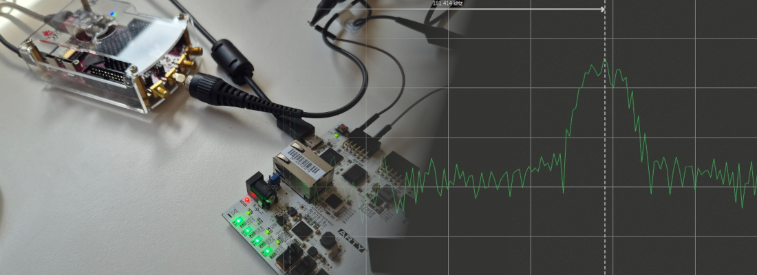
Once we have our model created, we can start with HDL Workflow Advisor. The HDL Workflow Advisor, according to its webpage, offers a workflow so that you can check your algorithm for HDL compatibility, generate HDL code, verify the code, and then deploy the code to your target platform. This tool uses several tools, one of these we have already seen on the blog, the FPGA Data Capture, but not only allows reading information from the FPGA but also allows writing on AXI4 Lite registers through the IP JTAG to AXI Master. To run HDL Workflow Advisor, first, we have to open the HDL Coder application from the APPS tab, and then, click on the Workflow Advisor button.

Once executed, a new window will be opened to configure the workflow we want to perform, in this case IP Core Generation, and the target platform. In my case, I going to use a Picozed 7015 board that previously I installed. The rest of the configurations will remain by default.

On the next step we have to turn on the option Insert JTAG MATLAB as AXI MASTER. This option will allow us to configure out IP through AXI4 Lite bus.

Next, on Target Interface we have to define which kind of interface we want to use for each port. In the case of the PMOD ports, we have to write the corresponding FPGA pin with the format {’PIN’}. Signals we want to connect o to FPGA data capture, the interface we have to select is FPGA Data capture – JTAG.
Another option to add a signal to FPGA Data Capture is by right click on the wire and enabling Test point.

In the next step, we have to select the clock frequency of our design. As we are using the Verilog Module from Digilent, we have to select a clock compatible with this module, and in this case, the module is designed to work at 22.59 Mhz, so the target Frequency selected will be configured on 22.6 MHz.

Next, we will jump to point 3.1.1, where we will configure Verilog as the language of the design.

The next point we will configure is point 3.2, where we will add the corresponding Verilog sources, and we will select the buffer size for the FPGA Data Capture. Also, we will check the box to enable the readback of the write registers. This option is only for debugging in our case, to ensure that the written value is correct.

Before continue, we have to delete the second line on the file axis_i2s2.v, since the code generated by MATLAB is not compatible with this line.
`default_nettype none
Finally, right-click on the 3.2.2 point and click on Run to selected task.

If all was good, all the steps will be executed without errors. The next is to create the Vivado project, generate and save the software interface, and generate the bitstream. All these steps are with the default options.

Finally, when the bitstream is generated, we can also program the board from this window.

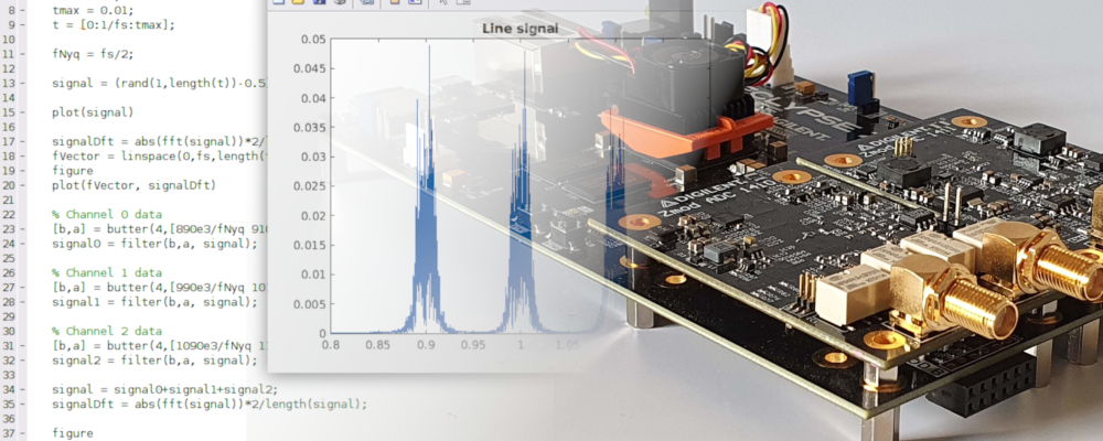
Now, we will verify the design. To write the AXI4 lite registers, I have generated this script that writes all the values with the selected ones. Filter coefficients are calculated with fir1 command.
close all
clear all
clc

%% Fir taps compute

taps = fir1(4,0.000001)

%% AXI registers configuration
h = aximaster('Xilinx')

enable = 1;

% FIR configuration
b0 = taps(1);
b1 = taps(2);
b2 = taps(3);
b3 = taps(4);
b4 = taps(5);

% Convert to fixed point
b0_qq = floor(b0*2^22);
b1_qq = floor(b1*2^22);
b2_qq = floor(b2*2^22);
b3_qq = floor(b3*2^22);
b4_qq = floor(b4*2^22);

% write AXI registers
h.writememory('40010118',0)

h.writememory('40010104',b0_qq)
h.writememory('40010108',b1_qq)
h.writememory('4001011C',b2_qq)
h.writememory('4001010C',b3_qq)
h.writememory('40010110',b4_qq)

h.writememory('40010118',enable)

release(h);
The algorithm will be verified through FPGA Data Capture, where we have stored the input and the output of the effect algorithm.
When I had the design finished, I noticed that the design doesn’t reach a soft clipping properly. That is because of the order of the filter since even though I design for a low cut frequency, the response of the FIR filter is limited. To get softer responses, we have several options, the easiest at this point is to increase the FIR order to 8, and add 4 more coefficients to the AXI interface. If this were a hard mission, we can change the type of filter to a 2nd order IIR filter with the same number of coefficients, and try to reach the desired response by changing Q and \(wc\).
In this case, I’m going to modify the FIR diagram to an 8th-order FIR filter, and I have assigned new AXI4 registers to the 4 new coefficients. On the script, the fir1 instruction has to be changed to an 8th-order filter, and the new coefficients have to be sent to the new addresses generated by MATLAB.

First, we test the output when the effect is disabled, and we can see how the output is the same signal as the output.

Next, I tested the design with 2 different types of clipping. First, with a high cut frequency, we can see how the design performs a hard clipping.


The next DFT diagram is corresponding with a lower cut frequency, which means a soft clipping. We can see how the high-frequency harmonics are attenuated by eliminating the high odd harmonics of the hard clipping; this is the same as saying that the signal is more sinusoidal.

[ ]
]
In this post, we have seen how to integrate an entire design on MATLAB from algorithm design and verify, integrate all the elements of the design through the use of Blackboxes, and then verify the response of the algorithm with FPGA Data Capture and the IP JTAG to AXI. It is very interesting how HDL Coder allows the designers to verify the signal processing algorithms with real signals, and then use all the MATLAB power to verify the behavior of the algorithm in detail. Also, is easy to perform changes at any step of the design, even when the design is in the verification process.