Running subcycle average models on Speedgoat Performance System (II).
 Speedgoat
In this post, we talked about the PWM signals, and how we can capture them to convert that discontinuous signal into a continuous signal. This process is called subcycle average. Now, how can we integrate the subcycle average in a power stage model? If we take the Buck converter model I used in other articles, the switch expects a boolean signal, so we cannot connect into the control port a single signal with a value between 0 and 1, so we need to use different blocks to create the Buck converter model. In this example, I have used an integrated Buck Converter block.

Opening the configuration of this block, we can find that we can select the Switching Device. This selection allows us to use different kinds of transistors, and a different configuration named Averaged Switch.

Using this configuration, the “gate” of the switching device becomes a continuous input where we can connect a signal with values between 0 and 1, exactly what we need. Notice that the time step of this block is \(tsm\), the time step of the model execution.

To connect the PWM Capture module, which runs at \(ts\), and the Buck converter model, we need to include Rate Converter blocks, configuring them with a time step of \(tsm\).

If we activate the timing legend on Simulink, we can differentiate two different time-step regions. The fastest region, which runs at \(ts\) includes the PWM capture, a Data Type Conversion block, and the Rate Converter.

And the slowest region that runs at \(tsm\) includes the Buck converter model and the IO334 conversions.

To test the model, I added a PWM generator with a Step block in the duty cycle input, and a Low-pass filter to smooth the duty cycle step.

To execute the model I have created the next script where I can modify the time steps and the PWM frequency to check the results. The duty cycle of the model is set initially at 20% with a step to 80% in t=0.2.
In the first test, I used a realistic scenario where the model was executed six times slower than the PWM capture.
clear all
close all
clc

Ts = 1e-6;
Tsm = 6e-6;

Fpwm = 100e3;
Tpwm = 1/Fpwm;
Vdc = 100;

sim("sca_buck_ss.slx")
In the vout response, we can see the fast artifacts of the converter like the step oscillation. Due to the oversampling performed by the PWM capture module, the ramp is shown as different steps.

Zooming into the signal, we can see that the PWM pu signal has an average of 0.8, and the output voltage has a value of 80 volts. Notice that the ripple in the Vout is missing.

In the next example, I have increased the \(tsm\) to 15us.
clear all
close all
clc

Ts = 1e-6;
Tsm = 15e-6;

Fpwm = 100e3;
Tpwm = 1/Fpwm;
Vdc = 100;

sim("sca_buck_ss.slx")
This time, we can see that the PWM pu signal is close to the average value. In reality, we are applying an average filter to the PWM signal so is normal that the signal will be close to its DC value.

Zooming into the signal we can see that the vout is pretty similar to the last one.

This time I have increased the value of \(tsm\), making the ratio \(tsm/T_{PWM}\) an integer value, so the value of the PWM pu will be always the average value. In this case, talking DSP, the signal is a multiple of the sampling frequency, so the image signal is located at DC.
clear all
close all
clc

Ts = 1e-6;
Tsm = 20e-6;

Fpwm = 100e3;
Tpwm = 1/Fpwm;
Vdc = 100;

sim("sca_buck_ss.slx")

Increasing the value of \(tsm\) will make us obtain different responses, in other words, the image signals will be located in different frequencies. This time, with a value of 23us, we can see how the ripple in the PWM pu signal is decreased with respect to 15 us.
clear all
close all
clc

Ts = 1e-6;
Tsm = 23e-6;

Fpwm = 100e3;
Tpwm = 1/Fpwm;
Vdc = 100;

sim("sca_buck_ss.slx")


Finally, if we increase the value of \(tsm\) to 100us, all the harmonics disappear, and the output of the model is a continuous signal. Even with this model, we will be able to test a DC regulator, but is true that we can find some issues in the dynamic response.
clear all
close all
clc

Ts = 1e-6;
Tsm = 100e-6;

Fpwm = 100e3;
Tpwm = 1/Fpwm;
Vdc = 100;

sim("sca_buck_ss.slx")

Now, is the time to deploy this model in the Speedgoat Performance, more specifically, we are going to deploy the model in the FPGA of the Speedgoat Performance. To do that, first, we need to make some changes to the model to make it compatible with the HDL generation. First, we need to change the solver of the Simscape model to Partitioning Solver.

This solver splits the model into different parts and uses different solvers for each one, represented by its state variable. Once the solver is updated, we need to update the model using Ctrl+D. Now, we can check which solver is used for each part of the model. This information is available on Debug > Simscape > Statistics viewer.

In my model, we can see that two different solvers are used, and we have linear and non-linear variables. In the Variables tab, we can check that the non-linear variables are related to the Buck Converter block used, specifically, they are related to the conductance (\(G\)) equations.
While solving non-linear equations is not a big deal for a desktop computer, Simulink cannot generate HDL code to solve this kind of equations. Fortunately, the Buck Converter block is prepared to be implemented in HDL, so we can change the value of Integer for piecewise constant approximation of gate input to a different value than zero. This will treat the conductance when the switch is saturated (\(G_{sat}\)) as a piecewise constant integer with a fixed range, which will linearize the conductance equation.
To make this change, we need to open the mask of the Buck Converter block and set the Integer for piecewise constant approximation of gate input to, for example, 10.

Now, if we compile the model, and re-check the partitioning, we will see that now, all the equations are linear, so the model is ready to be implemented in HDL.

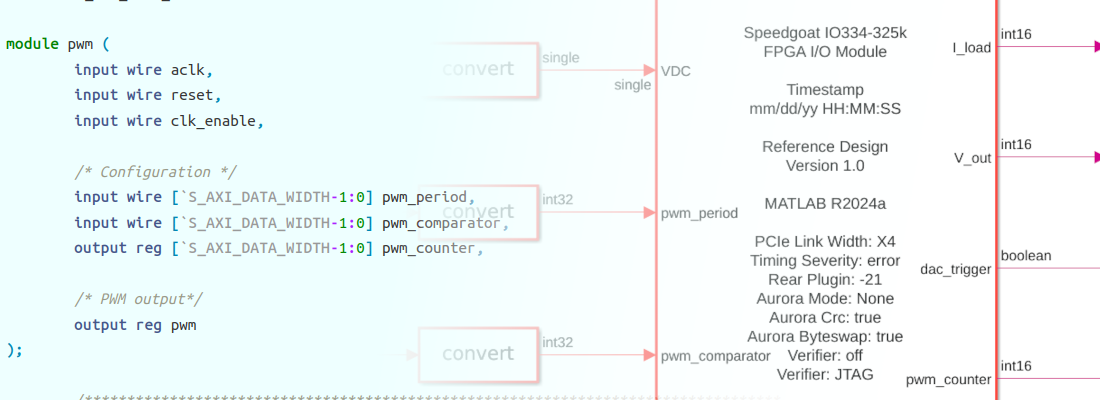
The complete model that we are going to deploy in the FPGA contains, in addition to the Buck model, the PWM capture block, the Rate Converter blocks and the gain blocks for the analog outputs.

On the top of the model where we had the PWM generation, we will have just the FPGA Block and the PWM generation we use in the simulation. Since the PWM input will be connected to a digital input of the IO334 we can comment out those blocks.

The next step is to generate the space-state model of the Simscape model. To generate this model, I have used the following script, which sets the number of iterations and enables the fixed cost.
sca_buck_ss_init;

open_system(['sca_buck_ss.slx']);
set_param(['sca_buck_ss/FPGA/Buck/Solver Configuration'],'DoFixedCost','on')

% Set number of solver iterations
set_param('sca_buck_ss/FPGA/Buck/Solver Configuration','MaxNonlinIter','2')

% Launch SS HDL advisor
sschdladvisor('sca_buck_ss')
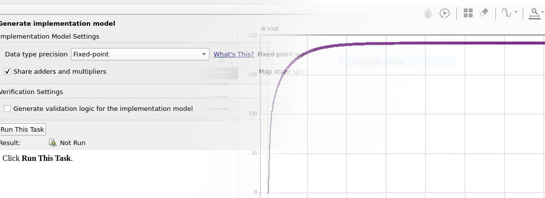
On the window that will be opened, we just have to click on Run All to generate the new model.

The generated model has the same behavior as the Simscape model but uses just math blocks. This model will be the one we use to generate the HDL code. From the generated model, we can make right-click on the FPGA block, and open the HDL Workflow Advisor.

The steps here are similar to the previous post. The following image shows the Set Interface Window of the HDL Workflow advisor.

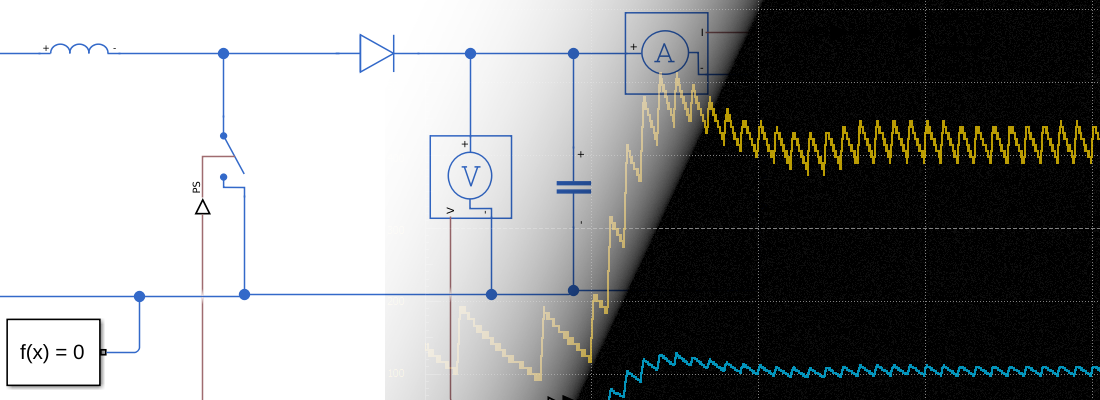
The subcycle average model I presented in this article uses the block Buck converter from the Simulink Simscape library, but sometimes we are working with a complex converter so we need to build the model using switches and passive elements. In these cases, we can use linearized switches to build the converter. Linearized switches are approximations of IGBTS or MOSFETS where gate input accepts values from 0 to 1. Simulink has a dedicated library for these elements. To open it you just have to execute SimscapeFPGAHIL_lib in the Matlab command window.

Opening them, we will see that the power side of the switch is the same for all the models, but the controller that sets the collector-emisor voltage, or the drain-source voltage for MOSFETs is what makes their behavior different. On the web, we can also find these models as Pejovic models.
To finish, I would like to mention that subcycle average models are not useful just for increasing the PWM frequencies. When we have a model in the FPGA that is controlled by a regulator that we are testing in the microprocessor, the output of the regulator is a continuous signal, so the model that runs in the FPGA has to accept continuous signals as control signals, so we need to use average models also in this case.
Subcycle average models are a tool that allows us to simulate any kind of model, even with high-speed switching frequencies, in a Speedgoat Performance. These models extract the essential behavior of the semiconductors and transform them into mathematical expressions that can be executed at high speed. The very good side of this method is that the fidelity of the model can be adjusted by modifying just the time-step at which is executed the model. The method has also limitations, and the most important is the aliasing. We have seen how making the time-step of the model a multiple of the PWM frequency all the ripple disappears. The key of all of this is that, if you have to use subcycle average you will be able to make your models faster, but you have to know what you are doing and, most importantly, the meaning of what you are obtaining.