Data acquisition from an electric model running on the FPGA of a Speedgoat Performance.
 Speedgoat
If there is a device that I would really like to have, it is a hardware-in-the-loop test system. These devices allow you to have almost any hardware circuit on your desktop with, in general, limited space. We already saw almost a year ago how we can deploy a hardware model in the Speedgoat Baseline, a device with a CPU and an FPGA. That device was great, but it was limited due to the speed of the FPGA and, especially, its size and ports. At that time we had an Artix7 50t, with 4 analog outputs, 4 analog inputs, and 14 digital IOs. That device was excellent for deploying little models or discovering what HIL is, and how it can help you. This time, Speedgoat has sent me its big brother, the Speedgoat Performance with the IO334 module and the IO3xx-21 plugin. the structure of this device is similar to the one I used before, the Speedgoat Baseline, but this time the device is more powerful in all aspects, from the CPU to the FPGA used, this time a Kintex7. Also, the IO capabilities have been increased, this time we have a 16-bit 16-channel DAC, and the same for ADC. In the IO3xx-21 plugin, we have 56 digital IOs configurable as input or output via software.

In this post, I will focus on data acquisition from a Buck converter simulation running on the FPGA. Differently from previous posts, I am using a Speedgoat Performance which allows me to use the CPU not just to configure and deploy the model but also to share real-time data with the FPGA.
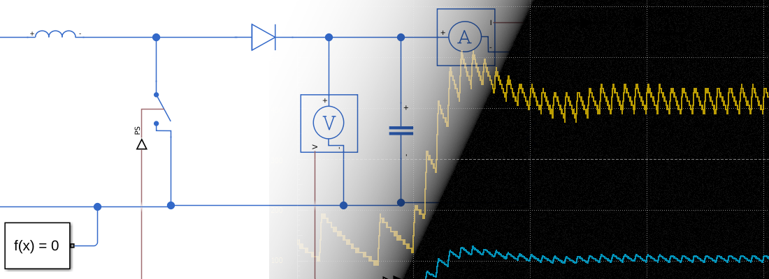
First of all, we need to implement the power electronics model. In this case, we are going to implement a Buck converter, as well as we did in the previous post using the Speedgoat. The only change I have introduced in the model is a series resistor in the inductor branch to reduce the overshoot when the input signal is not applied ramped. In this model, we are going to add some measurement blocks to read the values. These meters will measure the output current and the output voltage. Also, in input voltage will be generated by a controlled voltage source so we can modify the input voltage from outside of this model.

We also need to add a block to configure the solver of the model. In this block, we need to enable the use of a local solver and set the sample time as Ts.

The rest of the parameters of the model will be defined using the next script that we need to execute before any simulation or implementation. I always name this script as init_model.m
%% Model sampling time
Ts = 1e-6;

%% Model variables
L = 10e-6;
RL = 1e-3;
C = 200e-6;
Vdc = 100;
R_load = 2;
When the power electronics model is complete, we will put this model inside a hierarchy block. Now, we need to make the connection of the model to the digital inputs and analog outputs of the Speedgoat Performance. This device features an IO334 IO module with 16 analog outputs with a range of +-10V and a resolution of 16 bits, so we need to adapt the measures of the model to this range. A difference with the latest project, this time we are going to add each measure doubled. This way we can use one of them for visualization in an oscilloscope, and the other one to close the loop with the control device. Also, this will allow us to have different gains and ranges for visualization and control.
Once the connections for the external interfaces are completed, we need to add another interface to be connected to the PCIe bus. This interface will send data from the FPGA to the CPU so we will be able to plot data that is inside of the FPGA. For this project, we are going to send over the PCIe bus the output current and the output voltage. To do this, we need to know that the CPU can handle data slower than the FPGA, so the transactions can not be executed at every sampling step of the FPGA. To reduce the number of transactions we need to generate data packets of several samples, and then send the complete packet in just one transaction. This can be done using the block Tapped Delay. This block acts as a FIFO memory (also like a LIFO) with a configurable depth. Then, an enabled register in the output of the Tapped Delay will trigger the sending of the data to the CPU. The Enable input of the register will be connected to a trigger generation built with a ramp and a comparator. When the ramp reaches the depth configured in the Tapped Delays blocks, triggers the register and all the data is sent to the CPU. In the model we are designing, I have configured 100 samples, so the data will be sent in packets of 100 samples. This configuration, in the final design, is transparent to us, but we need to configure it well because a lower value in the configuration of samples can make the CPU isn’t capable to handle all the transactions, notice that a lower value indicates more transactions to send the same amount of data, and a high depth can’t be configured since there is a maximum amount of data for each transaction.

If you are using the HDL Coder Integration package for MATLAB 2023b or later, you can directly connect signals with “single” data-type to the analog interfaces. The int16 scaling is done under the hood, so the model can be simplified.
The MATLAB code that configures the gains is the next. This code will be added to the init_model.m file.
%% Gain configuration

max_dac_voltage = 10; % Visualization
dac_width = 16;

max_adc_voltage = 5; % Control

% Current
max_current = Vdc/R_load * 2;

current_gain_control = max_adc_voltage / max_current;
current_gain_control_dac = current_gain / max_adc_voltage * (2^(dac_width-1)-1)

current_gain_vis = max_dac_voltage / max_current;
current_gain_vis_dac = current_gain / max_dac_voltage * (2^(dac_width-1)-1)

% Voltage
max_output_voltage = Vdc;

voltage_gain_control = max_adc_voltage / max_output_voltage;
voltage_gain_control_adc = voltage_gain / max_dac_voltage * (2^(dac_width-1)-1)

voltage_gain_vis = max_dac_voltage / max_output_voltage;
voltage_gain_vis_adc = voltage_gain / max_dac_voltage * (2^(dac_width-1)-1)
This model will be the one implemented in the FPGA, so we need to configure the data formats according to the hardware. The PWM input will be boolean type while the input voltage will be configured from the CPU so it will be a floating point signal. Regarding the outputs, all of them will be connected to the DAC of the Speedgoat so all of them will be int16 for an HDL Coder Integration package older than 2023b, and just single for newer versions.
While the model running on MATLAB can handle the double precision data type, the model implemented in the FPGA can only handle single precision data type so, later we will need to change the data types of the analog ports. To make this easiest, we can add a block **Data Type Specification” on every analog port, so later, we can change the data type of these blocks using a script.
Finally, when the model is complete, we are going to generate the top model, which will be executed in the CPU. In this model, we will have the FPGA design in a hierarchical block, and then we are going to connect the inputs of the model to a generator. The input voltage signal will be connected to a Constant block with a fixed value configured in the init_model script. To test the model, we are going to generate a PWM input using the block PWM Generator.
For the output of the model, we need to undo the conversion for the DAC to obtain the real value of the output current and the output voltage. Regarding the PCIe Data output, they will be connected to a [File Log] block to be stored in a file. In addition, we need to add the block Enable File Log to start and stop the data logging. This is important because the amount of data can be huge for long simulations.

One can be tempted to think that, when the model is deployed in the FPGA, and the real-time model shows DAC outputs, they can be logged without the need for a Tapped Delay blocks, but this is not true because these outputs are connected to the DAC, not to the processor, so they cannot be reachable. Also, they are sampled at the sampling time of the FPGA, so they cannot be plotted using the processor without a big data loss.
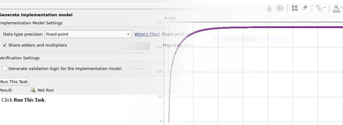
Once we have the model to be deployed in the Speedgoat complete, we can generate the implementation model. The next lines show the commands to generate this model. Is important to configure the parameter MaxNonlinIter, since it is closely related to the time step of the model once it is deployed.
open_system('buck_model');
set_param(['buck_model/FPGA/Buck/Solver Configuration'],'DoFixedCost','on')

% Set number of solver iterations
set_param('buck_model/FPGA/Buck/Solver Configuration','MaxNonlinIter','2')

% Launch SS HDL advisor
sschdladvisor('buck_model')
The execution of these lines will open the Simscape HDL Workflow Advisor window. To generate the model we can click on Run All.

I have noticed that in the latest versions of MATLAB, there is an extra step in this workflow that checks the target and the frequency of the device that we are going to use to deploy this model. If they are not defined, this workflow will return a Warning that can be ignored since the target and the frequency will be configured later. If you want a clean workflow, you can navigate to the HDL Configuration, and set the target as ASIC… and a target frequency of, in this case, 200 MHz. By doing this, the workflow will finish without errors or warnings.
When the implementation model is generated, (it has the prefix gm_*), we can execute a simulation and the results have to be similar to the next.

OK, now we are ready to deploy the model onto the Speedgoat. The first step is generating the model that will be implemented in the FPGA. To do that we will use HDL Coder and the HDL Workflow Advisor. The first we have to do is prepare the model to be converted into an HDL code. This process is written in the next script. We need to configure the Vivado version we are going to use, in this case, we need to use 2022.1. now we need to make some changes in the model, but these changes can be done automatically using the command hdlsetup. Next, we need to set as Single the analog inputs and outputs of the model. Remember that we mentioned this before.
%% Set Vivado version
hdlsetuptoolpath('ToolName','Xilinx Vivado','ToolPath','/media/pablo/data_m2/xilinx/Vivado/2022.1/bin/vivado');

open_system('./sschdl/buck_model/gmStateSpaceHDL_buck_model');
set_param('gmStateSpaceHDL_buck_model', 'SimulationCommand', 'Update')

hdlsetup('gmStateSpaceHDL_buck_model')

%% Set to single the model data types
set_param('gmStateSpaceHDL_buck_model/FPGA/Signal Specification','OutDataTypeStr','single');
set_param('gmStateSpaceHDL_buck_model/FPGA/Signal Specification1','OutDataTypeStr','single');
set_param('gmStateSpaceHDL_buck_model/FPGA/Signal Specification2','OutDataTypeStr','single');
set_param('gmStateSpaceHDL_buck_model/FPGA/Signal Specification3','OutDataTypeStr','single');

%% Configure and launch HDL Workflow Advisor
generate_hdlworkflow;
Finally, there is a function named generate_hdlworkflow. This function executes all the steps of the HDL WFA using a script. I have used this in this project since, if I have to repeat this process several times, now I just have to execute this script. if I use the GUI I have to set part of the configuration every time. To generate this script, you can generate it first using the GUI, and then, in the File menu, export it as script, so the next time you can generate the HDL code executing the script.
The script is available on my GitHub, but I want to mention some configurations that are important in this design.
The first one is the Oversampling factor. This number sets the ratio between the speed of the FPGA and the speed of the model. remember that the time step of the model is defined by the next equation.
So, If I want to reduce the time step, to improve the fidelity of the model, I can modify three different factors, the FPGA clock frequency, the oversampling factor, and the number of iterations. The FPGA clock frequency is configured at 200 Mhz, which is high enough for a Kintex7, so it is better not to increase it. The number of iterations is configured in two, which is small, and for some designs, we will obtain better results by increasing this number, so reducing it is not an option. Finally, the oversampling factor can be slightly reduced without many implications since the FPGA just needs some cycles to execute the PCIe transactions and mainly to perform single datatype math calculations. So, in case of the need to improve the fidelity of the model, oversampling will be the winner. For a first approximation, we are going to configure it in 100.
hdlset_param('gmStateSpaceHDL_buck_model', 'Oversampling', 100);
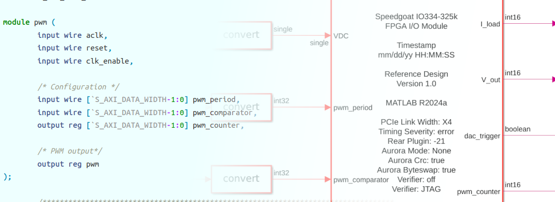
Now, we need to configure the parameters of the reference design. The device I have has the IO334 and also a Rear Plugin that manages the digital IOs, so we need to confirm it with the parameter 'RearPlugin','-21'
hdlset_param('gmStateSpaceHDL_buck_model', 'ReferenceDesignParameter', {'PCIe_Link_Width','X4','timingSeverity','warning','RearPlugin','-21','AuroraMode','None','AuroraCrc','true','AuroraByteswap','true','HDLVerifierAXI','off'});
Finally, another important configuration is the IO Interface Mapping. The output voltage and the output current will be connected to the IO334 AO Data interfaces, the PWM will be connected to the TTL IO3xx-21 interface, and the outputs and inputs that we want to manage from the CPU will be connected to the interface PCIe Interface. The code that executes this is the next.
% Set Inport HDL parameters
hdlset_param('gmStateSpaceHDL_buck_model/FPGA/Input voltage', 'IOInterface', 'PCIe Interface');
hdlset_param('gmStateSpaceHDL_buck_model/FPGA/Input voltage', 'IOInterfaceMapping', 'x"100"');

% Set Inport HDL parameters
hdlset_param('gmStateSpaceHDL_buck_model/FPGA/PWM', 'IOInterface', 'TTL IO3xx-21 [0:55]');
hdlset_param('gmStateSpaceHDL_buck_model/FPGA/PWM', 'IOInterfaceMapping', '[0]');

% Set SubSystem HDL parameters
hdlset_param('gmStateSpaceHDL_buck_model/FPGA/Buck/HDL Subsystem/HDL Algorithm/State Update/Multiply State', 'SharingFactor', 1);

% Set Outport HDL parameters
hdlset_param('gmStateSpaceHDL_buck_model/FPGA/DAC I output Vis', 'IOInterface', 'IO334 AO Data [0:15]');
hdlset_param('gmStateSpaceHDL_buck_model/FPGA/DAC I output Vis', 'IOInterfaceMapping', 'Channel 01');

% Set Outport HDL parameters
hdlset_param('gmStateSpaceHDL_buck_model/FPGA/DAC V output Vis', 'IOInterface', 'IO334 AO Data [0:15]');
hdlset_param('gmStateSpaceHDL_buck_model/FPGA/DAC V output Vis', 'IOInterfaceMapping', 'Channel 02');

% Set Outport HDL parameters
hdlset_param('gmStateSpaceHDL_buck_model/FPGA/DAC Trigger', 'IOInterface', 'IO334 AO Trigger [0:1]');
hdlset_param('gmStateSpaceHDL_buck_model/FPGA/DAC Trigger', 'IOInterfaceMapping', 'Channel 01 to 08');

% Set Outport HDL parameters
hdlset_param('gmStateSpaceHDL_buck_model/FPGA/DAC I output Control', 'IOInterface', 'IO334 AO Data [0:15]');
hdlset_param('gmStateSpaceHDL_buck_model/FPGA/DAC I output Control', 'IOInterfaceMapping', 'Channel 05');

% Set Outport HDL parameters
hdlset_param('gmStateSpaceHDL_buck_model/FPGA/DAC V output Control', 'IOInterface', 'IO334 AO Data [0:15]');
hdlset_param('gmStateSpaceHDL_buck_model/FPGA/DAC V output Control', 'IOInterfaceMapping', 'Channel 06');

% Set Outport HDL parameters
hdlset_param('gmStateSpaceHDL_buck_model/FPGA/PCIe Data', 'IOInterface', 'PCIe Interface');
When Vivado finishes the implementation of the model, MATLAB will generate a new model which will be executed in real-time. This model contains both the part that will be executed in the CPU and the part that is implemented and run in the FPGA. As I mentioned before, this model contains the analog outputs that will sent to the DAC, but this does not mean that this output could be read from this model. The same for the PWM input, since it is connected to the digital input blocks.
Even though the PWM input is not connected in this model, it contains a PWM Generator that will be compiled in this model, and it can have issues due to the sampling step, so we can comment (right-click on it > Comment Out) this block. Regarding the bus voltage, since its interface is PCIe Interface, we can modify its value and it will be sent to the FPGA. Regarding the output voltage and the output current, they will be sent over PCIe from the FPGA to the CPU, so we will be able to plot them without problems, considering that they are sent in bursts of 50 samples, so they are not shown in real-time.

A little configuration is needed in the File Log blocks to plot data well. We need to change the input processing of the blocks to Columns as channels (frame-based)

Also, the FPGA model allows some configuration. We cannot change the model that is running, but we can change the configuration of the DAC and the digital inputs. We can access this configuration by double-clicking in the FPGA block.
On the analog output side, we can configure the output range of the channels. Consider that the value we send to the DAC is the number of counts, not the output voltage.

On the digital input side, we can configure the voltage of the port, and also if the port has a pull-up resistor or not, and the voltage that is connected to that pull-up.

Regarding data logging, since the simulation can be long, or even with an infinite duration, we need to configure the amount of data, and when we want to save the data. All of this will be done with the Enable File Log block. In this first case, a simple step is connected to the block, so the model will log data during the time that this step value is one, then when the step value is zero, the log is deactivated.

One thing that makes this tool very powerful is that we can use any schema in the enable signal, for example, if we want to capture an event that occurs between run time seconds two and three, we can create more complex triggers.

Before launching the simulation, we need to change the time step of the model to 50 microseconds, since the part of the model that is executed in the CPU cannot be executed at the initial time step which was 1 microsecond.
Ts = 50e-6;
Now, we are ready to launch the simulation. I used in this project first the Arty board, to check that all is well connected, and then the ZUBoard with a custom SYZYGY module that features a 4-channel ADC with an input range of +-10V, and 4 digital outputs. The design running on this board is quite simple. It just has a PWM modulator and a simple low-speed closed-loop control to keep the output voltage in a valid range.


When we launch a simulation, we will see in the MATLAB workspace that a new variable is created. This variable contains the data of the logs. Performing a step from 10% to 80% we can see the response of the model in the logged data.

Also, since I have configured two different outputs for the output voltage and the output current, we can connect the other output to the RedPitaya STEMlab to see the response.

In the above capture, we can see the output voltage in green and the output current in yellow. We can see that there is a low-frequency harmonic in the simulation. After many checks, I realized that this oscillation was due to the aliasing. I mentioned before that the time step of the model depends on the FPGA clock, 200 Mhz in this case, the oversampling factor, configured in 100, and the iterations of the solver, configured in 2, so the time step of the model was 1 microsecond. This time step, for the switching frequency I selected, was not small enough to represent well all the harmonics of the output voltage and current, so I decided to reduce the time step to 0.5us by changing the oversampling factor to 50. With this change, the low-frequency harmonic was reduced enough.


The power of devices like the Speedgoart performance comes from its heterogeneity. It features a fast FPGA that can execute models with very small time steps, a powerful CPU able to handle data from the FPGA and in which we can modify the design as in the desktop computer, and finally, a set of IO modules connected to the FPGA with high bandwidth. The best is that all of them can work separately, but also together in the same model to improve the fidelity of the model or make the developer’s life easier. In a model, each device fits in a different part of the model, in this case, the simulation of the power stage needs to run fast, however, the generation of the input voltage or the logging do not have to be fast, but they need to be configured in the execution time. Ultimately, developers have very similar tasks compared to working with a Zynq MPSOC, where we need to separate the tasks between the FPGA, the APU, and the RPU.