Getting started with ZuBoard and Petalinux
 ZUBoard
In the last post we talked about the possibilities that working with a Zynq MPSOC device offers us. Also, on LinkedIn, there was a conversation about the new roles that the industry will need to work with complex devices that feature different architectures inside, a kind of “SoC Architect” (name invented by me). This new role will have to split the tasks into the different architectures. This new role will need knowledge, not necessarily deeply, about the strengths and weaknesses of all the architectures inside the SoC, and it has to select the best one to execute different tasks. A long time ago, many people said that technology would destroy jobs because of automation, what they didn’t know was that many new jobs would be created, the difference is that these new roles require knowledge.
This article is a new article in the Getting Started with Zynq series where I develop basic designs with Zynq devices. This time we are going to use a Zynq MPSOC device. The board I going to use is the AVNET’s ZUBoard. This board features a ZYnq MPSOC 1CG, the smallest device of the MPSOC family and a very good option if you are working with Zynq 7020 and you need more power in the application processor.
CG parts are a subset of the MPSOC devices that feature a dual-core ARM Cortex A53 at up to 1.3 GHz. As a real-time unit they feature a dual-core ARM Cortex R5 at 533 MHz. A strength of all the MPSOC families is that all of them have Gigabit transceivers in the APU, so we can connect PCI devices like SSD, SGMII, Displayport…

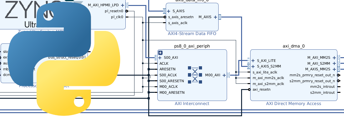
Zynq MPSOC devices, like all other Zynq devices, feature an FPGA (Programmable Logic, PL). MPSOC devices have different AXI interfaces to send data from the PS to the PL and also several interfaces to send data from PL to PS. For the HW design, we will use Vivado. Later, for the SW design we will use Vitis, either to develop applications in bare-metal or applications that will run in Linux.
The first step will be the HW definition of our project. As we mentioned before, for the HW project we will use Vivado, so we need to create a new project on Vivado. The name I chose is “zuboard_base”.

In the project creation wizard, we need to select the part we are using or the board we are using. If we are using a commercial board, is pretty sure that it will be included in the Xilinx boards repository, so we just need to introduce the name of the board and it will appear to be selected. If the board is not downloaded yet, we can do it by clicking in the download button. Now when the board is downloaded, we can select it and continue.

Once the project is created, when we are working with Zynq devices, in general, we will work using a Block Design, so the next step is creating a new block design.

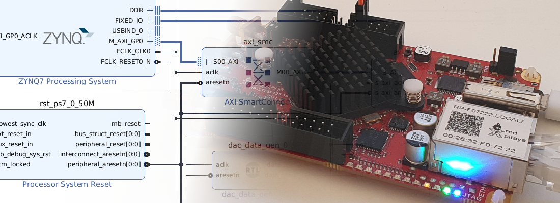
When the block design is created, we can add the Zynq device in order to configure the Processing System (PS). When we execute this step, Vivado will add a generic PS without any configuration about the DDR or the peripherals. To apply the configuration of the board, a pop-up will appear. When we apply the configuration to the board, remember activate the tick Apply Board Preset. Once we have done this, the PS will be configured according to the board we selected in the last step.

Applying a board preset does not mean that the configuration is fixed, we can access the configuration of the PS by double-clicking on the Processing System, and the configuration window will be opened. Here we can find a diagram of the device where we can check the available and the enabled peripherals, APU characteristics, internal connections…
If we have selected a board, the enabled peripherals will be those that the board manufacturer has used in the board. If the board has external connectors, like the ZUBoard with the SYZYGY and the Click socket, maybe some of them are not enabled by default. Also can be possible that the connectors use pins from the PL, so we will need to add a controller IP to manage this connection. For example, in the ZUBoard, the Click socket has dedicated pins for SPI, I2C or UART, but they are connected to the PL, so we will need to add an IP to manage that interface.

If we come back to the block design, on the left we can open the Board tab, where we can find the elements we can add to the block design that are pre-configured. To add these peripherals we just need to drag and drop the one selected.

Now we can see how a controller IP is added to the block design. These IP are managed through AXI4, so they need to be connected to the interface. This task can be automated yes by Vivado by clicking on the pop-up. Now, Vivado will ask us to which interface we want to connect the new IPs. Since both used interfaces are equivalent, for this design Vivado will select the first one. Also, it will add a reset for the IP, generated by the PS reset, and an AXI Interconnect that acts as a switch for the several IPs. The complete block design will be the next.

Once we have the block design complete, we need to create an equivalent RTL code from the block design. This equivalent RTL is named Wrapper, and it can be generated by cliking on Generate HDL Wrapper.

At this point, we have a synthesizable HDL code, so we just need to generate the bitstream.
Finally, when the bitstream is generated, the next step is the SW development. To do this, we need to generate a file that connects the HW design with the SW development. This file is the .xsa. The xsa file is a compressed file that contains the bitstream, needed to configure the PL, and some files with information about the configuration of the PS like peripherals enabled, addresses of the PL peripherals, PLL configurations… We can generate this file by executing Export hardware on Vivado.

At this point, we finished the HW design (regardless of debugging iterations), so we are ready to start developing the SW development. With the xsa file, we can develop a bare-metal application or build a Petalinux distribution. These devices are very useful when we run Linus in the APU and a bare-metal application in the RPU as we did here.