The art of sharing
Again, you are reading the first post of the year, there are three of these posts for now, and the show will go on. For the first post of 2024, I am going to publish an article that explains a talk that I presented at a conference, but they rejected it, so since I already had some images and the content prepared, let’s go. The title of the article does not clarify the content of the article but this is because that is just the title of the talk, and is the subtitle that gives some sense to the article: The art of sharing. Execution of DSP algorithms in Zynq MPSOC. The idea of this talk, now article, is to present how we can use efficiently the resources of a Zynq MPSOC device when we have to execute DSP algorithms.
In the beginning, when processors had just one core, and with luck, a floating point unit (FPU), there was just one way to execute the algorithm, in the only core. At that time, this article had no sense but then, manufacturers started to print in the same die more than one core for a CPU, and this brought us the twice power but also made that we needed to face access to resources that were not doubled, in other words, we needed to share resources (see how the title of the talk, now article, begins to make sense). When all indicated that the peak of the power had been reached, the manufacturers became crazy and doubled again the number of cores, and a few years later, they introduced different devices in the same core, and finally, they introduced all of these different devices into an FPGA, and Zynq MPSOC was born. Later they continued increasing the complexity by interconnecting all of them with a Network on chip (NOC), and Versal was born, but that is another talk…
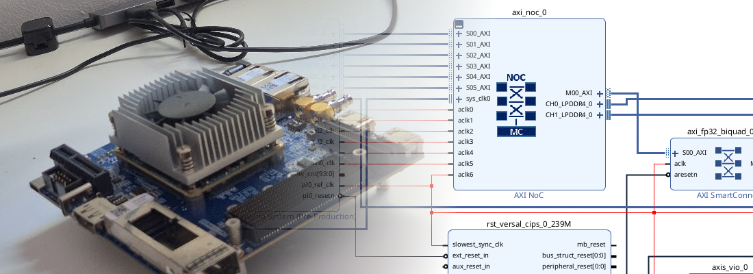
Focusing on Zynq MPSOC, these complex devices feature three different devices inside. First of all, we have an ARM Cortex A53 (Application Processing Unit or APU) with two or four cores, then we have an ARM Cortex R5 (Real-time Processing Unit or RPU) with two cores, and finally an FPGA. In this scenario, and the task to execute a DSP algorithm using this device, the first that comes to your mind will be… WTF? You have three different devices, three powerful devices capable of executing your algorithm by far, even blinking three different LEDs while the algorithm is executed. In this talk, now article, I am going to present you up to four different ways to execute your algorithm, and this will be valid also for artificial intelligence, or any other algorithm.

In the majority of the algorithms, this will operate on a data set, so where that data is stored, or read, will determine the way we will execute the algorithm. Regarding the data storage, on Zynq MPSOC we have three different kinds of memories, four if we count the FPGA block RAM. The first one, the main memory, the external DDR managed by the DDR memory Controller. This memory can be read and written by any of the three devices. The APU and the RPU have direct access, and the FPGA has access through the DMA, so the DDR will be interesting storage to share data. The second memory is the On-Chip Memory (OCM). This memory is inside the chip and its size is 256 KB. It is clocked with the same clock as the RPU, what means that it is very close to it, becoming the path between the RPU and the OCM in a low latency path. In addition, the OCM can also be accessed by the APU. Finally, we have the Tightly Coupled Memory (TCM). This memory is connected just, and directly to the RPU. Actually, we have four of these memories, each one with 64 kB of space, and two of them are connected to the first core of the RPU, and the other pair is connected to the second core. These memories are not accessible directly from the APU since, as I mentioned, they are connected to the RPU, but the APU can access to them through the RPU. It is interesting how these memories have different addresses according to the device that is accessing them (TCM Memory Map).

After this introduction about the places where we can store data on Zynq MPSOC, the first way of executing a DSP algorithm on this device is acquiring that data, or signal, on the FPGA (or Peripheral Logic, PL), and sending that signal to the DDR using the DMA channels. Acquiring data from the PL is very interesting, especially because of the speed. Although APU and RPU are really fast, the speed that interfaces such as SPI can achieve is limited. Also, when we are working with high-speed ADCs, they usually use interfaces that are not included in regular processors like custom serial interfaces, or JESD204, so using the PL for this purpose is almost mandatory. In this kind of structure, we also need speed in the data sending from the PL to the DDR, and that speed can only be guaranteed if the processor remains outside these transactions. I don’t have nothing against the processors, they are great at sending “Hello world” over UART, but in case of high-speed acquisition, FPGAs are always the best choice. Using the DMA, we ensure that the signal is sent to the DDR at the speed of the FPGA. If the signal we want to capture is even faster than the DDR, we can add a FIFO in the DMA path to have a buffer where samples are stored before they are sent to the DDR.

In this structure, the DSP algorithm would be executed in the processor. Once all the signal is stored in the DDR, the FPGA raises an interruption to the APU or the RPU to indicate that data is ready to be processed. Since data is stored, and later processed, we can’t use this structure for algorithms that require running in real-time, for example, a signal that is filtered to be used in motor control. This structure will be very useful to, for example, check the integrity of a signal to generate metrics. Notice that the APUis designed to run a high-end operating system such as Linux, so using one or more core of it to run algorithms could be inefficient. For that purpose, Zynq MPSOC also features the RPU, a dual-core ARM Cortex R5. This processor has also direct access to the DDR, so using it to execute a DSP algorithm over data that is stored in the DDR is as fast as do it from the APU. The only difference is the speed. While the APU runs up to 1.5 GHz, the RPU is limited to 600 MHz, which is fast enough to run any DSP algorithm.

For now, we used the FPGA just to acquire the signal, but if we are working with RF signals or any signal above 0.5 GHz, we will face many problems executing any algorithm in real-time, so we just have one choice, execute it in the FPGA. In the next two structures, both the acquisition and the processing are executed in the FPGA. Many times, the processing that we execute in the FPGA is just a pre-processing such as demodulation to bring the signal to base-band and reduce its frequency. In the next structure we will find that the APU is the receptor of the signal. In this case, if the APU is running Linux, we can run into jitter problems since some system interrupts could delay the algorithm execution.

To avoid the jitter in the algorithms tasks, we can use a real-time operating system (RTOS), either in the APU or in the RPU, although as I said before, is better to reserve the APU for high-level tasks. This kind of operating systems allow us to control precisely when the tasks are executed but forget to use it to execute DSP algorithms in real-time with fast signals. Usually, the time step of this operating systems is between 1 ms and 10 ms, they allow us to execute a task with a period of 1 ms, which is enough to execute, for example, a stream of audio samples.
In addition, if we use the RPU, we can replace the DDR with the TCM, so we will take advantage of the low latency path between the RPU and the TCMs.

In summary, using complex devices such as Zynq MPSOC or even Zynq7000, adds an extra step in the design process. We not only have to design and implement the algorithm but also select the best device in which to execute it. Honestly, having different options to execute an algorithm is the type of decision that I would like to take in many other fields.