Using PS clocks for your PL designs
 ZUBoard
Sometimes people who want to start in the FPGA world ask me for a recommendation of a development board to start with. My answer to this question is always a Zynq board for several reasons. First, maybe they are not interested now in using the PS of a Zynq, but if they still improving their skills in FPGA, in short place they may need to use an AXI4 interface, or even run Linux on the board. The second reason is the cost. Now, we can find boards with Zynq as cheap as boards with an Artix7 FPGA. A very interesting board for this purpose is the AVNET ZUBoard, a board that features a Zynq MPSOC 1CG with a cost of less than 200€.
The problem with these boards is that, if you want to create a design just for the FPGA, you don’t have a clock connected to an FPGA pin, so you have two options, or your design is completely combinational, or you will need a clock. In this article, we are going through this problem, and we will see how we can use the Processing System clock generators for the Peripheral Logic
First. we are going to create a project as usual. We need to add the corresponding Verilog files to the project, in my case, I am going to use the boost converter model.

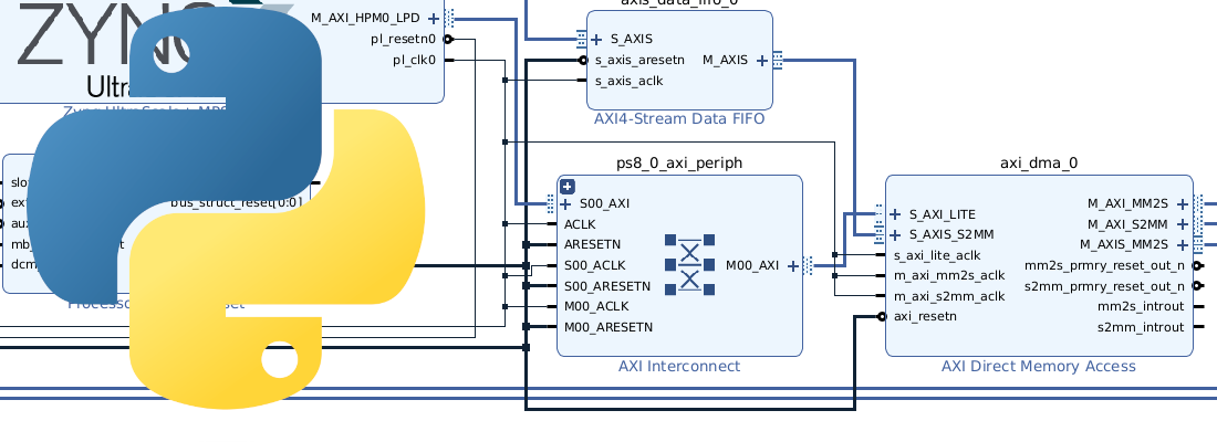
Since we will use the Processing System to generate the clocks, the easy way to do this is by using the block design. If you already have a top file written in Verilog or VHDL, you can add directly the top file to the block design. In the block design, we are going to add all the modules needed for the design. Also, we can connect them, except for the clock and the reset signals.

At this point, VIvado is asking us to Run Connection Automation assistant, but since there is not a clock in the board, it just will add an input for the clock and another input for the reset. At this point we need a clock source and also a reset source, so we are going to add the Processing system.
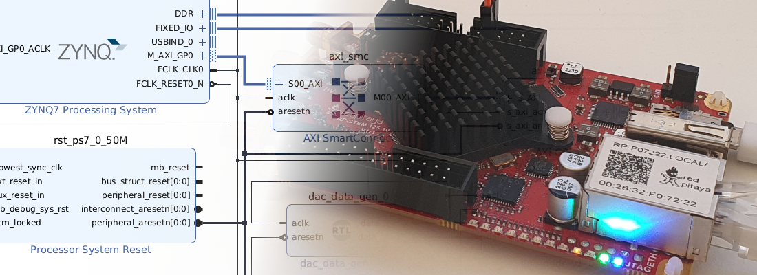
Once the processing system is added, we can disable all the peripherals of the PS since we are not going to use the processing system itself but just the PLL. To configure the PS PLL, we need to customize the PS and navigate to Clock Configuration. Then, in the tab Output Clocks, under PL Fabric Clocks we can find the output clocks we have available. four in this case. In this window, we can also configure the output frequency and which PLL we want to use. I always use the IOPLL since it lets me achieve the desired frequency more precisely.

When the output clock is enabled, in the block design we can now connect the clock and the reset signals to the PS generated. With these connections, the block design is complete.

The boost converter model has an external input that has to be connected to a pin of the board, For this article I am using the ZUBoard from AVNET, and it has a Mikro Bus Click connector, with a PWM input, so it will be that input which I will use for the PWM input of the converter.
set_property PACKAGE_PIN G6 [get_ports S1_pwm]
set_property IOSTANDARD LVCMOS18 [get_ports S1_pwm]
Now, we can generate the bitstream.
The next step in a regular FPGA design, will be sending that bitstream to the board and it will work, but this time is different. The clock in this design is generated by the processing system, but it is not configured in principle, so all its peripherals are not running. To make the PLL run, we need to configure the PS by sending it an application. The content of the application does not matter, even it can be just a while loop, the key is that the PS is configured.
The flow to configure the PS is the same as follows to run an application, first we need to export the hardware in Vivado, and then use that xsa file to generate a new platform.

Now, we need to add an Application project to the workspace. I have used the Hello World application from the Vitis examples.

Next, we can build and Debug the application in the ZUBoard. Now, when the debug session starts, the program pointer will be initialized at the top of the Hello World application, but before, all the peripherals of the PS, including the PLL have been initialized, so the clock must be running now.

To verify that the clock is running, in the PL design I added an ILA to check the model outputs, and we can see in Vivado that the ILA is running correctly.

Another option to have a clock in the PL of the ZUBoard is connecting a clock to the SYZYGY connector that has several clock pins, but this requires a SYZYGY board design. Other boards like the Picozed FMC carrier v2, in addition to the clock connected to the PS, also have a clock connected directly to the PL, so you don’t have this problem, but in general, manufacturers just want to include one clock. Fortunately, Zynq devices are very versatile, so you will have almost always a workaround for problems like this.