Using FPGA Data Capture to debug a design.
In the project developed in this post, to verify the behavior of the filter, we used the data acquired from the ILA. Data were processed on MATLAB with a script where we read the CSV, and verify input and output signals. This process works, but MATLAB gives us the choice to integrate the verification process also in the MATLAB workflow. To do that, we have to add a new module on our block design that will make the function of the ILA, with the advantage that MATLAB can require the data directly to this module without Vivado. The tool I will show you on this post is FPGA Data Capture.
If we check the official webpage of the product, we can see that MATLAB offers us 2 different workflows to use FPGA Data Capture. The first one is based on the HDL Coder Workflow, where the entire process, from design definition, to project creation is made inside MATLAB. This process is preferred if we have a supported hardware platform, and we want to develop a probe of concept. The second workflow MATLAB offers us is based on adding a Data Capture IP to our existing design. This way is what we will use on this post, since we have a design, and the goal of this post is to verify its correct behavior.

Our background is the next. We have a design already implemented and we want to verify its behavior. As we know, a great disadvantage of the FPGA is debugging. If we are working with a microcontroller, access to its memory to verify the result of an algorithm, or the output of a filter, is very easy, the only thing we have to do is connect a JTAG, and from an IDE we can see the value of the different memory positions. In the case of the FPGA, the debug process starts on the design, due to the debugging, or verification of an FPGA design will be a part of the design, unlike the microcontrollers, where debugging is executed in parallel in our application. At this point, even if we had a design complete, we will have to modify the design to integrate the verification modules, so, that is what we will do.
The FPGA Data Capture module is generated on MATLAB executing on the command window the instruction generateFPGADataCaptureIP.

When we execute this command, a new window will be open to configure which data we will capture, how is that data, and the length we want to capture. This window is pretty similar to Vivado ILA capture configuration but has a great difference.

If we expand the Sample depth field, we can see that the amount of data that can be configured to acquire is up to 1 million samples, unlike the ILA blocks where the number of samples is limited to 100 kilo samples. Notice that this number of samples will be stored on BRAM, so the amount of BRAM available in our design must be greater than the amount used to debug.
For this design, the clock of the system is running at 100MHz, with a data rate of 10Mhz, and the interest signal is centered on 1MHz, with a swing of 200kHz. With this, we can configure a sample depth of 1024 points, which will be enough to see 100 cycles, which is enough to verify the filter response. As the width of the filter input is 14, and the filter output is 18, the memory used in this design will be around 32kb.
Once the configuration is done, and we have chosen a name for the IP, and the folder we can click on Generate button.

A new folder will be created with the Verilog or VHDL files that we have to add to our Vivado project. Also, a Simulink model and two MATLAB scripts are generated:
- datacapture_model.slx. This model can be used to acquire FPGA data from a Simulink model and process data inside Simulink.
- launchDataCaptureApp.m. MATLAB Script to open a tool where we can start the acquisition manually. Data will be stored on workspace.
- datacapture.m. Script to acquire data directly from MATLAB commands.

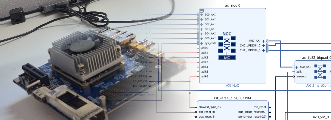
Next step is integrating FPGA Data Capture IP in our Vivado design. To do that, first, we have to open the Vivado project. On shared files, you can regenerate the project by executing the script line_filtering.tcl.
Before executing the script, we have to add all FPGA Data Capture IP files to the project, by adding the next lines to the script. First, we will define the path to the Verilog files:
set projectDir ../../projectset projectName eclypsez7_fir_plnx_2020.1
set bdName eclypsez7_fir_bd
set srdDir ../../src
set xdcDir ../../xdc
set memDir ../../memory_content
set bdDir ../../script/2020.1/bd
set dtDir ../../../hdlsrc_datacapture
Next, we will add all Verilog files to the project
## Adding verilog files
add_file [glob $srdDir/cen_generator_v1_0.v]
add_file [glob $srdDir/butterbp.v]
add_file [glob $dtDir/*.v]
Now we can save the modified file with a new name and execute it.
A new Vivado window will be opened with the last project, and the data capture files added. On block design, we can delete the ILA module, add the new Data Capture module, connect, and generate the bitstream.

Also, we can save the new block design with the TCL command.
write_bd_tcl /home/pablo/git/line_filtering/vivado/script/2020.1/bd/bd_line_filtering_datacapture.tcl
When the bitstream is generated, we have to program the device. Once the device is programmed, is important to close the HW server from Vivado, since the JTAG will be used by MATLAB, and we need Vivado to leave the JTAG.
Now we return to MATLAB, and as I said before, there are 3 ways to access the FPGA Data capture IP. To verify the filter, I have configured my signal generator to generate a white noise signal, so the DFT of the output of the filter has to be corresponding with its bode diagram. First, we can check if data is captured correctly with the FPGA Data Capture GUI. To open this window, we have to execute the script launchDataCaptureApp.m. Once the window is opened, we can configure the trigger position and the trigger condition, and the name of the variable where data will be exported into the workspace. Also, on the Data Types tab, we can configure the data type for each signal.

When we have all configured, we can click over the Capture Data button. At this point, when a trigger event will occur, data will appear on the Logic Analyzer window. On this window we can see, 2 signals where we can see capture information (number of capture windows and the trigger position), and the rest of signals are the configured. In our case, filter input and output.

Also, a Simulink model is created with some elements added. First, we can see a block named From FPGA, which is the interface block between the host, and the Data Capture Ip inside the FPGA. Signals that we can connect from this block are the same as we can see on the Logic Analyzer window. A simple model is shown in the next image, where I have changed the scope by 2 display blocks, where we can see the Capture window number and the trigger position of this capture, and the signals connected to 2 convert blocks, connected to a Spectrum analyzer.

Last, we can manage the capture directly from MATLAB command Window. To do that, I have written a script that computes the DFT of the filter’s input and output and then compares them.
On the script, first, we need to read the data on the FPGA data Capture IP, and according to the file datacapture.m, we can perform this with the command step, and the object datacapture.
dco = datacapture;
dco.setDataType('filter_input',numerictype(1,14,13));
dco.setDataType('filter_output',numerictype(1,18,13));
[Capture_Window,Trigger_Position,filter_input,filter_output]=step(dco);
Besides the read command, I have added 2 lines to set the corresponding numeric type to the signals. When data is captured, we can plot the input and the output of the filter.

Now, to verify the behavior of the filter, on MATLAB we are going to compute the DFT of these two signals, and we can see that the filter has high attenuation on bands different from 1MHz.

In the post, we have seen how MATLAB can help us to debug a design. GUI tool is very easy to use, and gives us an interface similar to the Vivado Logic analyzer, with the advantage that, once captured, the signal is stored on a variable on the workspace. We can do the same from Vivado, as we can see in this post, but this method will make us save time. Also, if you want to automatize the process of the design verification, you have 2 options, first, you can design a model where your design will be verified, or you can create a MATLAB script to perform the verification, and both will be valid.