Designing a filter on MATLAB and verifying it using FPGA-in-the-loop and Eclypse Z7
If I say “software for engineering”, most of you probably think of MATLAB. I don’t know if there is any field in engineering which does not have a package in MATLAB, and digital signal processing and FPGA design are certainly not among them. The package Signal processing Toolbox will give us all the functions that we will need to design a filter or any signal processing system, Fixed-Point Designer allow us to quantize the data in our application and to verify the response on a digital system, and packages like HDL Coder and HDL Verifier will allow us to test our design using a real FPGA, and implement the system on our FPGA board.
In this project, we are going to design a filter with the help of the Filter Designer tool. That filter will be quantified according to the capabilities of our Zmod Scope 1410 board, which we will use to acquire our signal. At this point, we have to verify if the quantized model meets the defined criteria. Then we can simulate the quantized filter with a demo signal in Simulink. Next, we will generate the HDL code of the filter designed, and we will test this HDL code on the Eclypse Z7 board. While we still use our demo signal, the filter will run on an FPGA-in-the-Loop. This will give us information of the behavior of the filter in the real application. Then we will add the HDL code of the filter to our Vivado design and test the integration of the filter with the rest of the design. Finally, we will verify the behavior with the Zmod AWG 1411 and the tool FPGA Data Capture.
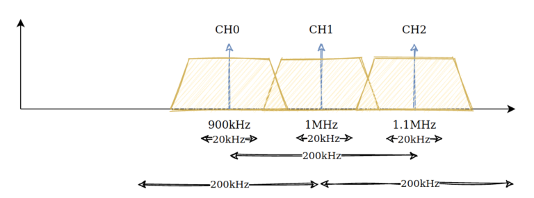
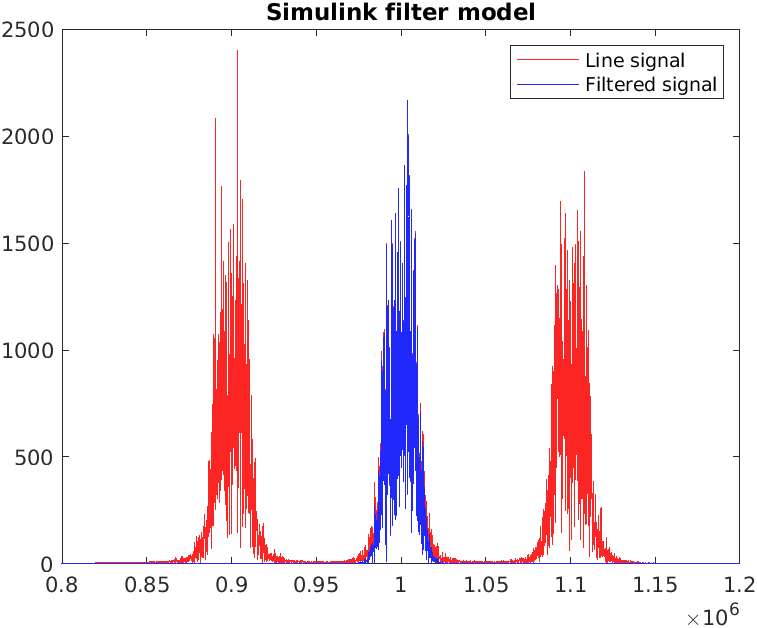
The application we are going to design is a decoder. It is very common to share the same transmission line to transfer different types of data, or even to transfer power. The way to transfer data without interfering with other kinds of data is to split transfers in different channels, but if only one channel is available, the way to do that is to split the frequency spectrum (frequency division multiplexing). That technique has been used for a long time to transmit different radio stations over the same data line, the air. Another example is PLC (Power Line Communication), where we can transfer power, at frequencies of 50Hz or 60Hz, and data, at frequencies of several hundred kilohertz. To get the frequency band of interest, we have to extract it and to discard the others. Once all data is transferred, we need to extract the range of frequencies that we have assigned and discard the rest. For that, we will need a bandpass filter. The frequency spectrum of our transmission line is shown in the next figure. Each channel has a bandwidth of 20kHz, and the space between channels is 100kHz.
To avoid interferences, we need to ensure an attenuation of at least -60dB on the bandwidth of the other channels. The filter we are going to design will obtain the signal from channel 1, so our filter needs the following characteristics:
| f (kHz) | dB |
|---|---|
| 910 | -60 |
| 990 | 0 |
| 1010 | 0 |
| 1090 | -60 |
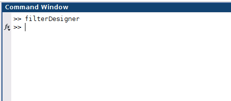
To design the filter, we will first open Filter Designer tool.
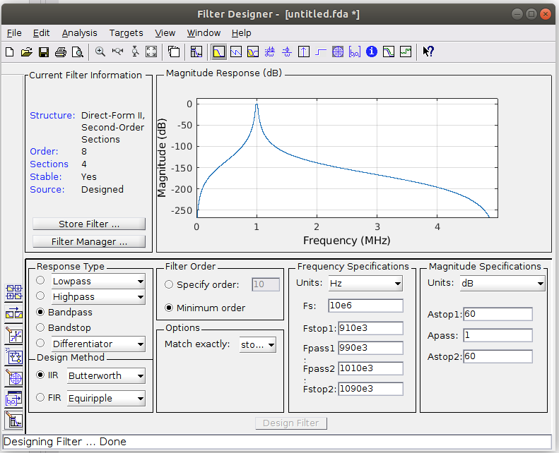
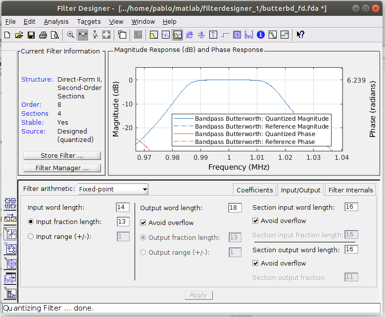
This tool allows us to configure all the characteristics of our filter. For this design, we will select a bandpass IIR (Infinite Impulse Response) Butterworth filter, because it allows us to create a low-order filter with high attenuation, and it has a fairly flat passband. Once we entered our frequency specifications, clicking on Design Filter will update the filter response.
Once the filter is designed, we can export it to our workspace. For that, select File > Export, and export it as an object.
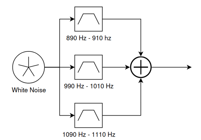
To test the correct behavior of the filter, we need to generate a signal that contains the three bands of frequencies. In the next diagram, we can see how this signal is generated using a white noise signal generator and three bandpass filters.
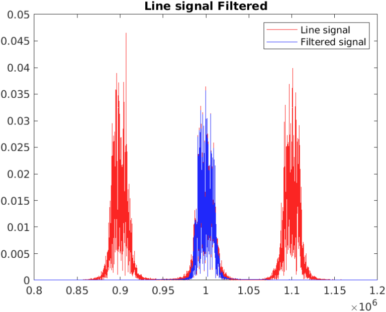
The next figure shows us the DFT (Discrete Fourier Transformation) of the entire line (red) and the response of our filter (blue).
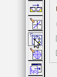
Once the filter is verified, the next is to quantize the filter according to our acquisition system. For our example, we will use the Eclypse Z7 Zynq-7000 SoC FPGA board and a ZMOD Scope 1410. The output of the AD9648-105 analog-to-digital converter (ADC) on the ZMOD Scope has a maximum sampling rate of 105 MSPS, but for our design, a sample rate of 10 MSPS is sufficient. The data width of our output is 14 bits. With these parameters, we can configure the quantization by clicking on the button with the stairs.
Then click on Filter Arithmetic, and more options will show. There are 3 tabs, one to configure the width of the coefficients, one for the width of the input and output, and the last to configure the width of the internal data of the filter.
Input and output widths have to be selected according to the input and output data in our design. The tool has a very interesting option that allows to let MATLAB select the fractional part of the output to avoid overflow. In our case, if we select 14 bits on input and output, we will see that the fractional part of the output is reduced to 9. This will cause a loss of the resolution of the filter, and this also means that output, at some point, can take values of up to +/-8 (3 bits). In our case, as the gain of the filter is 1, and to avoid base transformations in our FPGA design, we are going to select an output of 18 bits to keep the resolution of the output. We have to keep this in mind, because in our design, in case that the output of the filter exceeds the value of 1, we will need to add a saturation on the output of the filter.
Once we have the filter designed and quantified, we can export this filter to a Simulink model by clicking on Realize Model.
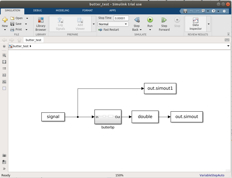
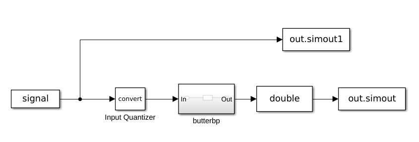
A Simulink window will open with the filter model already added. Now we can test the quantized model with the same signal we used to verify the continuous model. For this, we have to connect a From Workspace block to the input of the filter and to connect it to the signal variable. At the output of the filter, we will add a To Workspace block to save the data in our workspace. Remember that the filter output is quantized, so we need to add a Convert module between the output of the filter and the To Workspace block.
Executing the model and plotting the signals, we will see the following result:
Now that we have verified the filter with MATLAB and Simulink, we can generate the HDL code to test the filter on the Eclypse Z7 board.
To generate the HDL code, we have to make a change to the Simulink model first. When the filter model is inserted into the Simulink model, MATLAB adds a subsystem that contains a Biquad block, that corresponds to the filter, and a Convert block to convert a double signal to a quantized signal. Since we are going to generate the HDL code of the entire subsystem, we need to delete the Convert module of the subsystem and copy it into the main model.
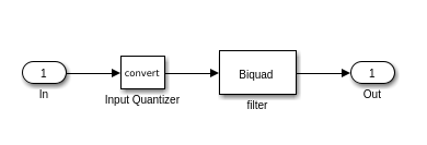
The next figure will show what the main model will look like.
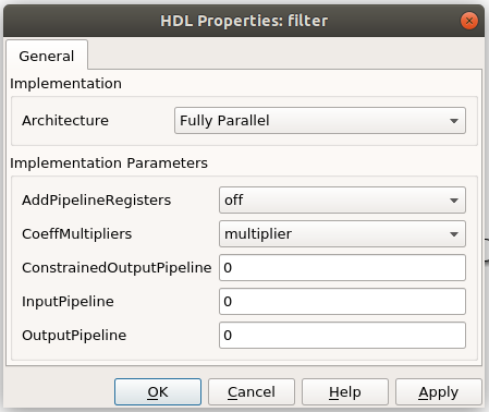
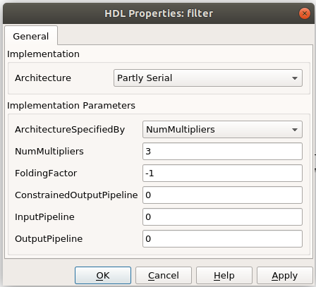
When the model has been modified, we have to configure the HDL implementation of the filter in the filter subsystem. Inside the filter subsystem, right click on Biquad block and select HDL Code > HDL Block Properties. A window like in the next figure will appear. In this window, we can configure the pipeline registers and the architecture in terms of multipliers used. We can choose between three different architectures:
- Fully Parallel architecture, where each multiplication of the filter will use one DSP Slice of the FPGA, and the output data frequency can be the same as the clock frequency.
- Fully serial architecture, where only one DSP Slice will be used. This architecture is the best in terms of DSP used, but all the logic added to manage the DSP Slice pipeline can increase the FPGA occupied slices. Also, the output frequency will be reduced to clk/multiplications. The reason is that for computing one sample, the design must perform ‘x’ multiplications using only one DSP Slice, so all the multiplications are queued. This configuration introduces new terms: Folding and Folding Factor. Folding is basically adding a multiplexer from n to 1 at the input of the multiply-accumulator block, where n is the number of multiplications that our filter has to execute. Using this configuration on MATLAB, the folding factor is maximum, and the throughput is low.
Partially serial architecture is in the middle. In this configuration, we can select the number of DSP Slices we want to use, or the folding factor. The throughput of the system will vary according to these settings. The disadvantage of this architecture is the use of logic increases.
To make the right choice, we have to think about our design. In our case, the input data has a sample rate of 10MHz, and the clock of the design will be 100MH. This means that we have 10 clock cycles between two samples, so we can only perform 10 multiplications. To compute a filter of the order 8, we need 16 multiplications, rendering the Fully Serial configuration useless. The Partly Serial configuration is useful if we don’t have enough DSP Slices available in our FPGA, but that is not the case in our example. So, the Fully Parallel architecture is the architecture of choice. Regarding pipeline registers, it is safe to assume that there will be no timing problems, so we don’t need to add them.
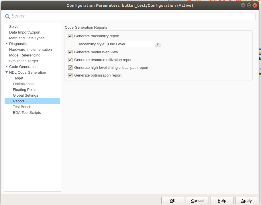
Now on the main model, right-click on the filter subsystem and select HDL Code > HDL Coder Properties. In this window, we can select the target HDL language and the device we will use. On the Global Settings tab, select the reset type. In our case, we need to select a synchronous reset. And lastly, on the Report tab, we will select all reports, so we can check our implementation.
When all the configurations are done, right-click on the filter subsystem and select Generate HDL for Subsystem. This step may cause errors if your Simulink model uses the blocks To Workspace and From Workspace. To avoid these errors, you can copy the filter subsystem and the input Convert block to a new Simulink model. This resolves the errors.
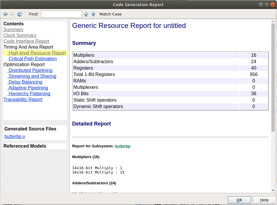
Once the HDL code is generated, the Code Generation Report window will show. If we open the High-Level Resource Report, we can see that our design uses 16 multipliers.
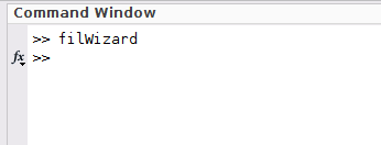
At this point, we have the HDL code of our filter, and as the next step, we will perform another simulation. This time, the filter will be executed on the FPGA. For this, we will use the FPGA-in-the-loop (FIL) module. To start this simulation, we have to open the filWizard tool from the command window.
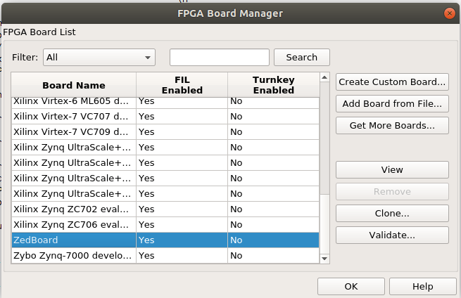
First, we need to create the board definition, which will allow us to connect the board through the FIL module. For this, we have to click on Launch Board Manager in the window showing. There we search for the ZedBoard since it is based on the same FPGA as Eclypse Z7 board. Then click on Clone…
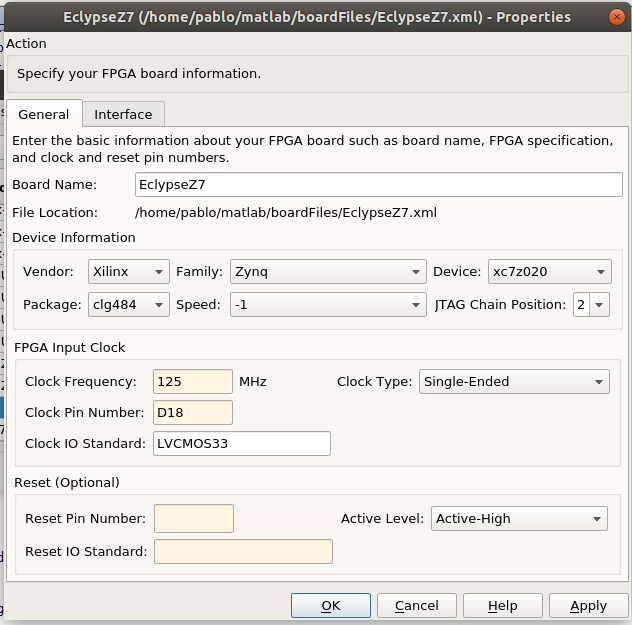
As soon as we entered the name and the location of the xml file for the board, a configuration window will open. Since our board is cloned from the ZedBoard, all the fields of the new window are already populated, but we need to change the fields that are related directly to the board, like clock and reset. In the case of Eclypse Z7 board, the clock source connected to the Programmable Logic (PL), is generated by the Ethernet PHY, has a frequency of 125MHz, and is connected to pin D18. The Eclypse Z7 board has no dedicated reset button. This is not a problem because it is not needed for the creation of a FIL board.
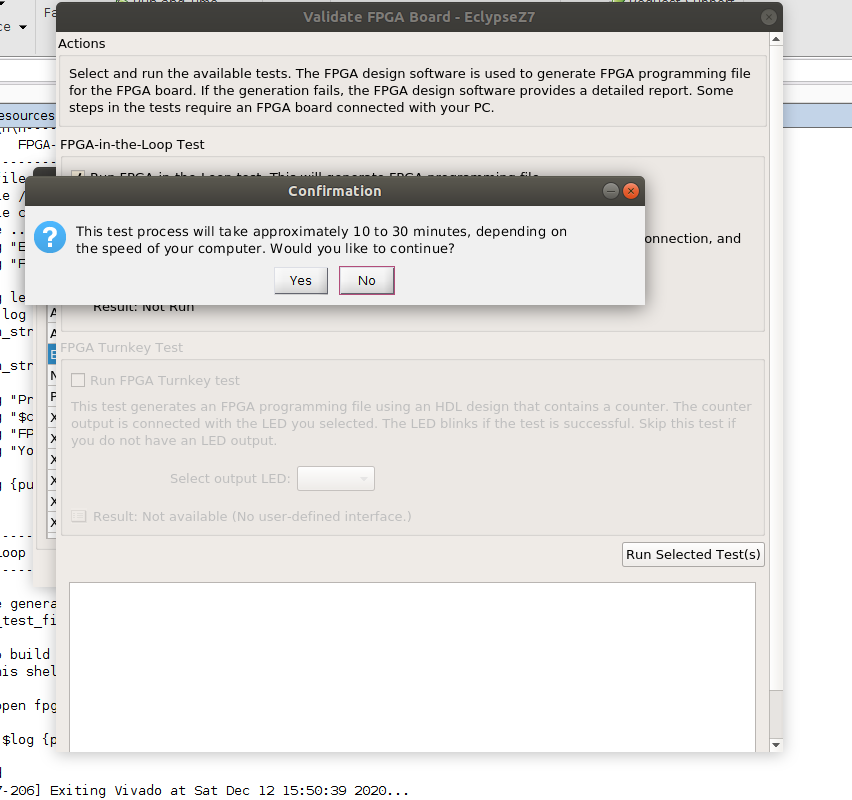
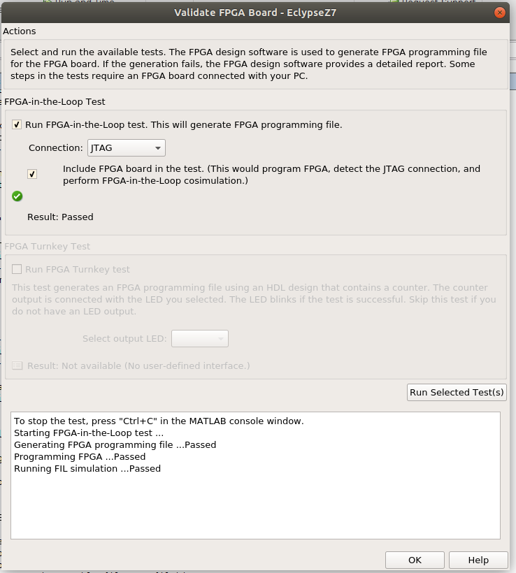
When we finished the definition of the board, we can click on OK, and we can select the board from the list. The next step is to validate the connection to the board. If we click on Validate, a new window will open. Here we have to configure the connection as JTAG, and we have to check the box to include the board in the test. When we click on Run Selected Test(s), a pop-up dialog will advise us that the test can take up to 30 minutes. We continue by clicking on Yes, and Vivado will be opened from the MATLAB command window, and it will start to synthesize and implement the FIL demo design.
If the test failed, the MATLAB command window might display a message that will ask for the Digilent Adept software.
To fix that, we have to download the Digilent Adept Runtime from Digilent’s webpage. Once it is installed, the validation will pass.
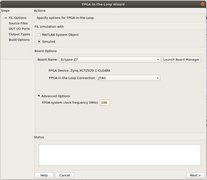
Now, on the initial Fil Wizard Board, we can select our new EclypseZ7 board and the connection to the board. In our case, only the JTAG connection is available, and the speed for the main clock of the FIL simulation
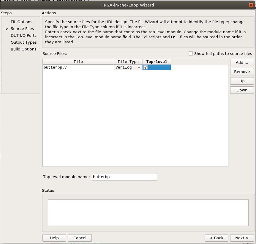
By clicking on Next, the following window will ask us for the HDL files. In our example, we will add the HDL with the fully parallel implementation, and we will indicate that the filter is the top level.
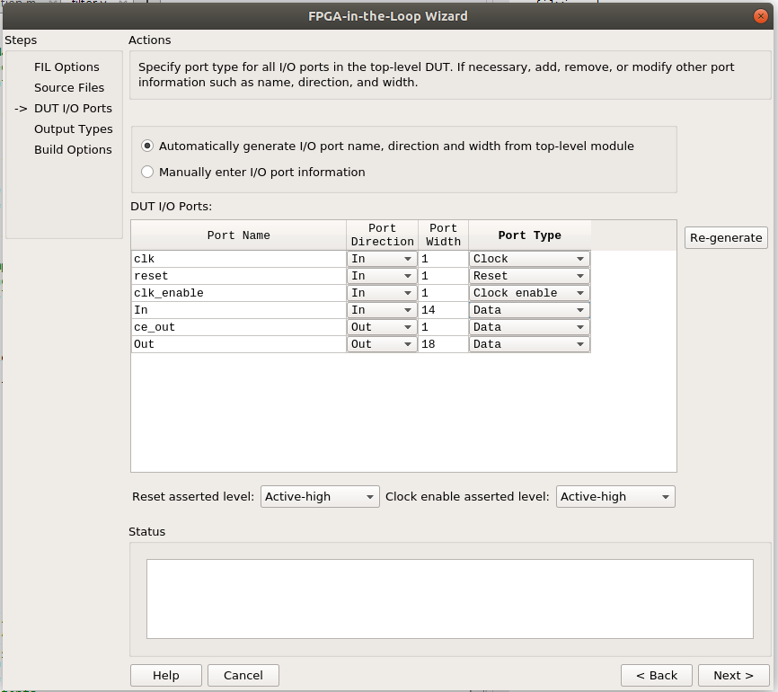
MATLAB will parse our file or files looking for the ports, clock signals and reset signal and show us the results.
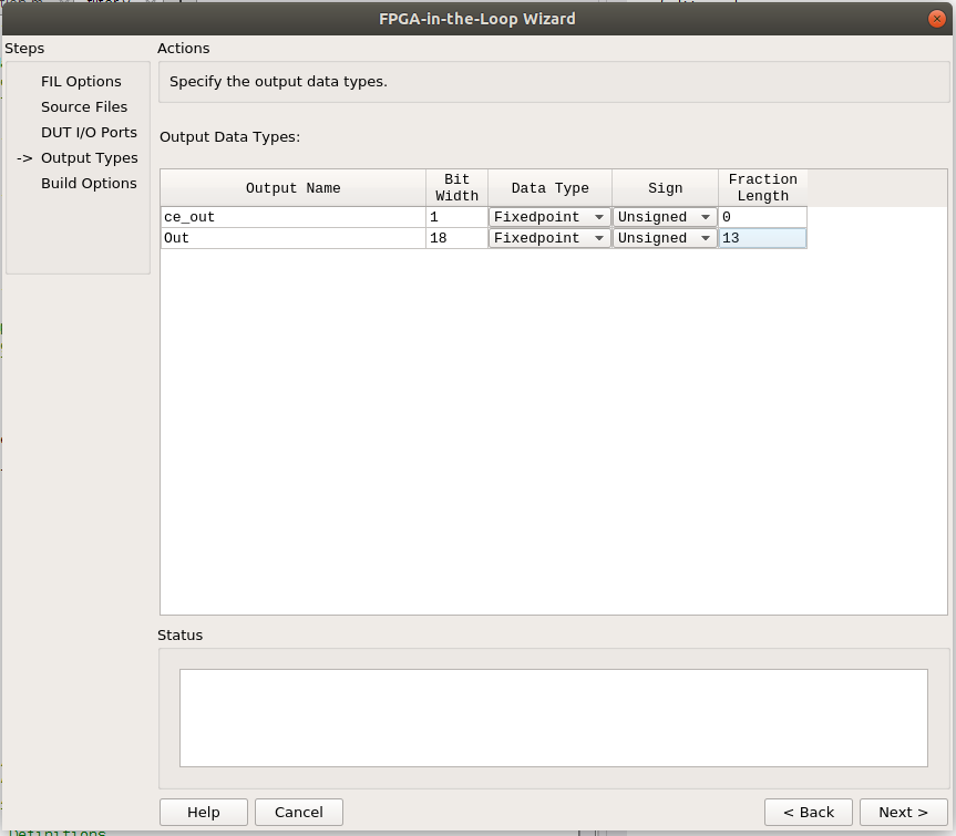
In the next window, we have to configure the format of the output data. This step is needed to see the output results on Simulink correctly. In our case, output data has a width of 18 bits, and the fractional part is 13. Notice that the sign by default is unsigned, and for our output signal that is wrong. The correct configuration is signed.
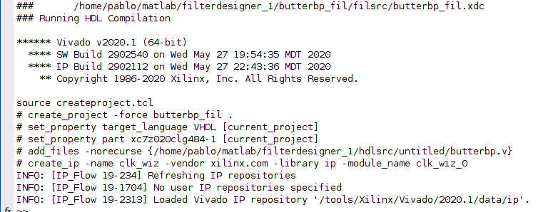
Finally, MATLAB shows us a summary of the project, and clicking on Build, Vivado will be opened in TCL mode and the HDL compilation starts.
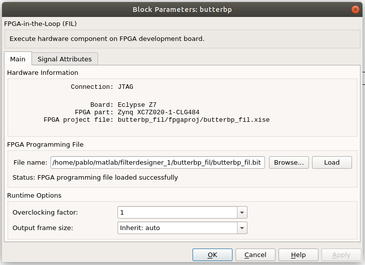
After Vivado has finished the synthesis, a Simulink model will open with the FIL block added.
Now, we can physically connect our Eclypse Z7 board, open the FIL model and by clicking on Load, the model will be loaded into the FPGA.
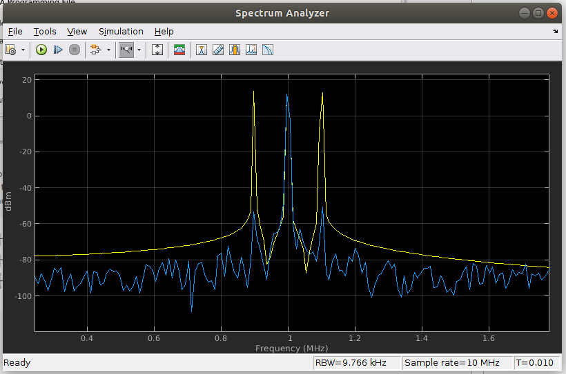
In the model we use to perform this simulation, we need to add 3 sine signals representing the 3 bands in our transmission line. The frequencies of these signals are 900kHz, 1MHz and 1.1MHz. To verify the output, we need to add a Spectrum analyzer.
Once the simulation finishes, the output of the spectrum analyzer will look like the figure following. We see 3 peaks at 900kHz, 1Mhz and 1.1MHz in the input signal, but the output contains only the 1MHz signal.
With this done, we have tested our filter and we have verified it on the FPGA. The next step is to create a design where we use this filter with a real analog input.
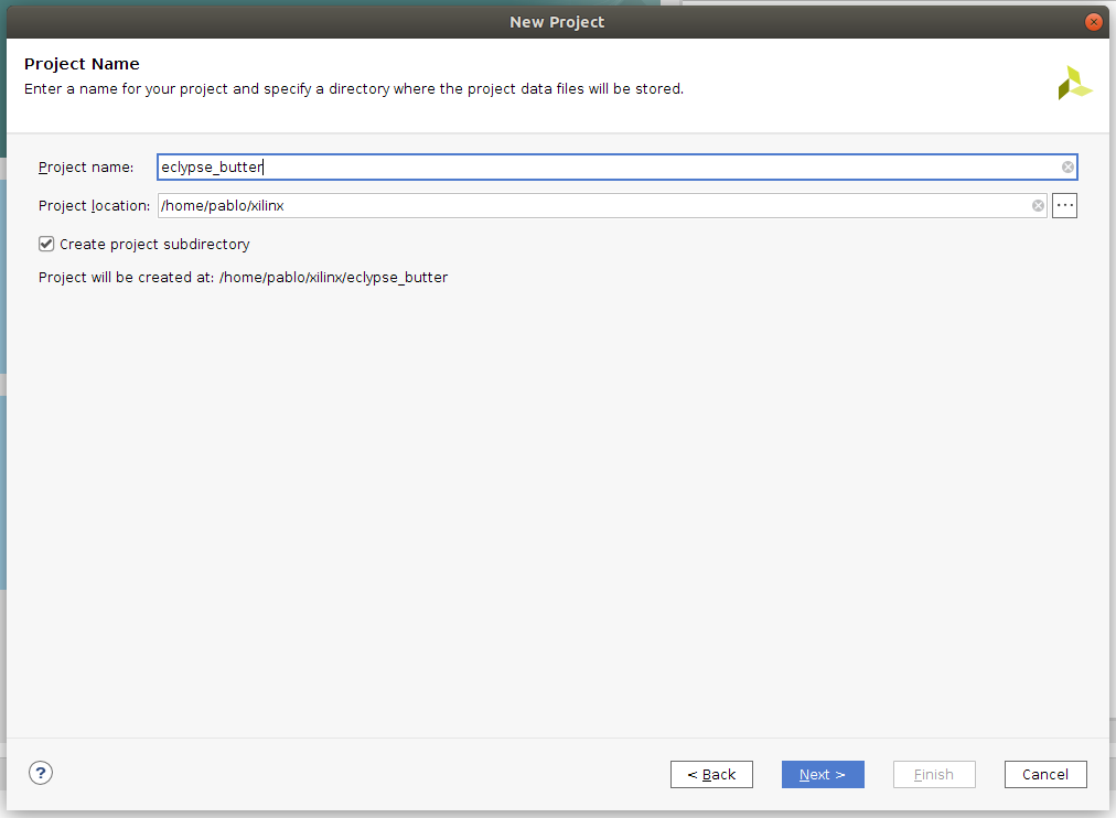
For this, we have to create a project in Vivado, which we name eclypse_butter.
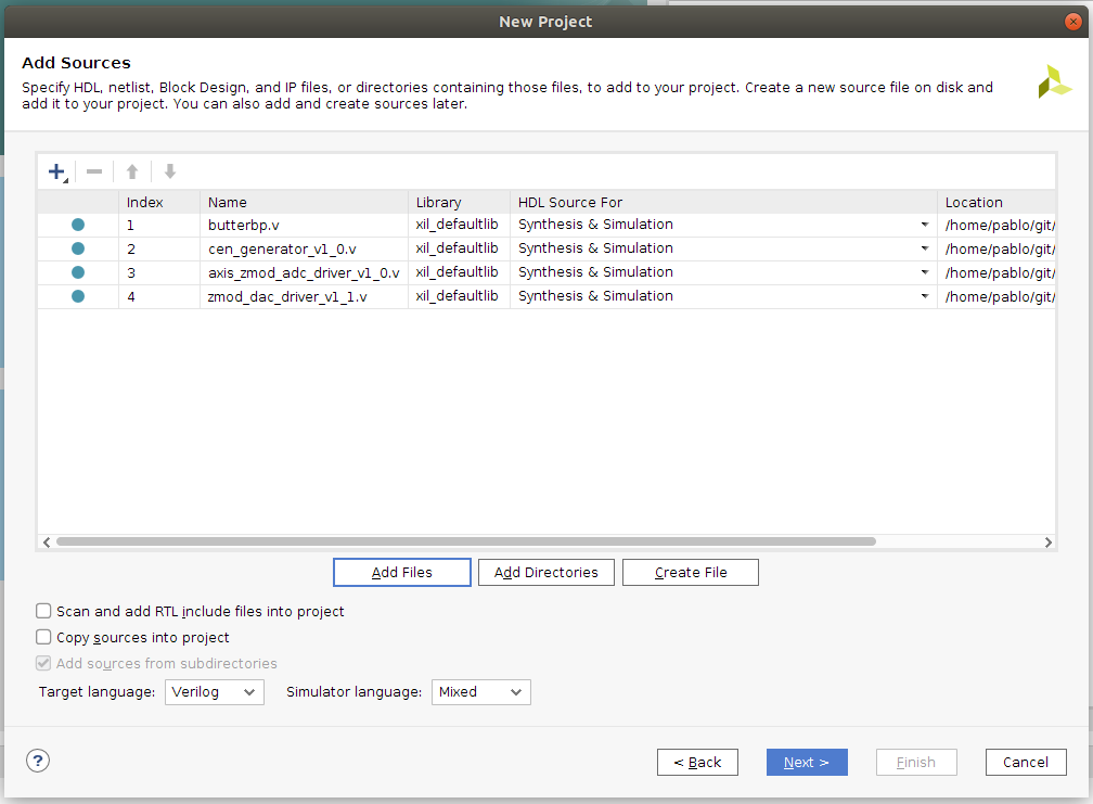
We need to add some sources to our design. First, we have to add the filter that MATLAB has generated (butterbp.v). Next, we need to add a clock-enable generator, since our filter works at a sampling rate of 10MHz, but our system clock is configured to be 100MHz. Also, the ADC and DAC drivers will be included.
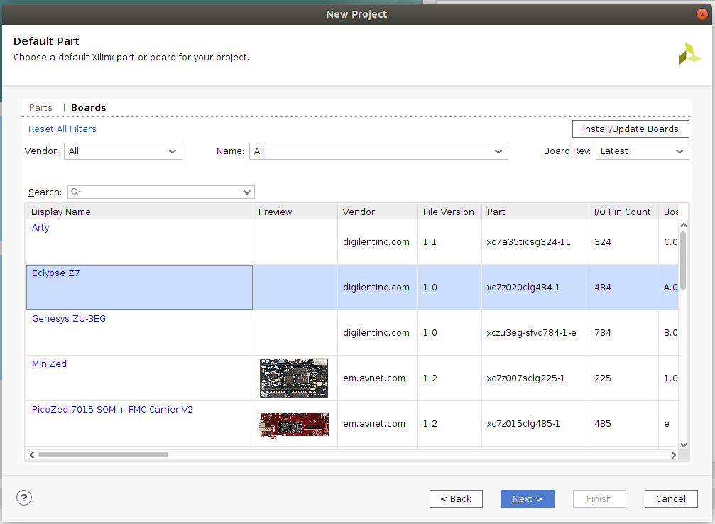
Regarding the board, we will select Eclypse Z7 board, which you can download from Digilent’s GitHub.
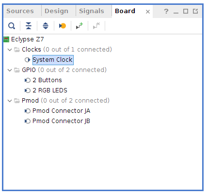
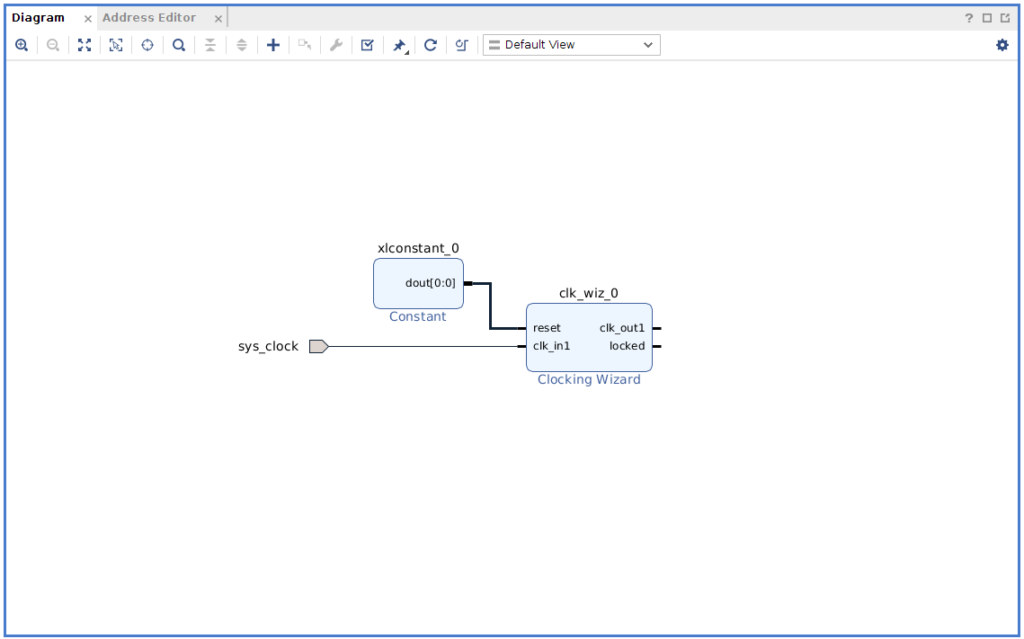
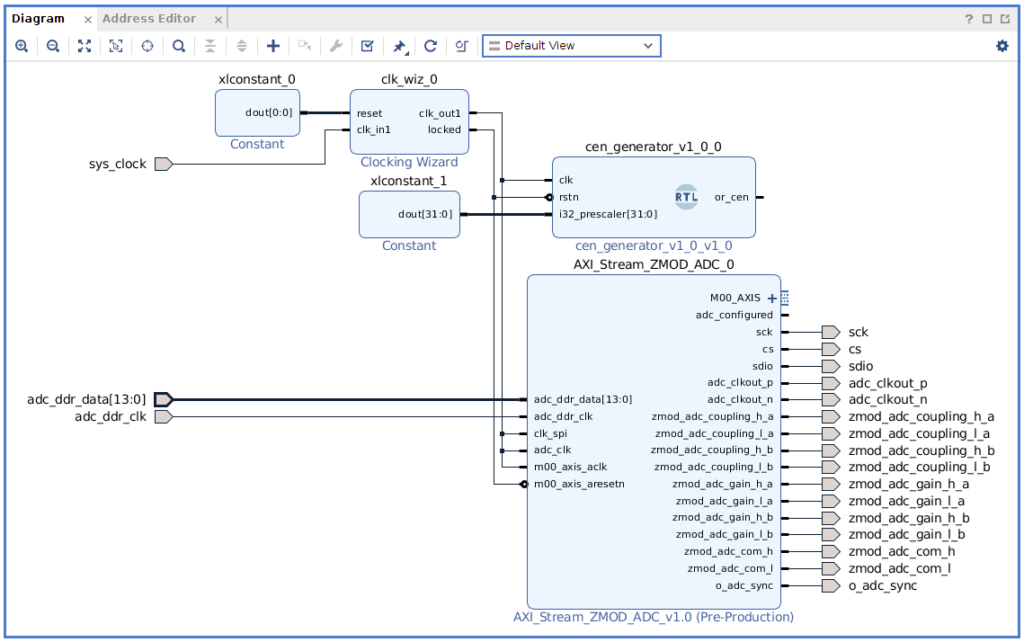
Once we have our project ready, we have to create a block design. It is a good practice when using the Eclypse Z7 board to add the Zynq block first. Our design uses only the PL. In other words, we are going to use the Zynq as an FPGA. The fact that the Zynq block is not in our design requires that the clock source for our design must be supplied externally. On the Eclypse Z7 board, there a 125 MHz clock connected to the PL from the Ethernet PHY, and this is the clock we will use. To do that, we can add the element System Clocking on Board tab. This element will add to our block design a Clock Wizard.
As we don’t need a reset pin, the reset input of the Clocking Wizard will be connected to a constant block with the value ‘0’.
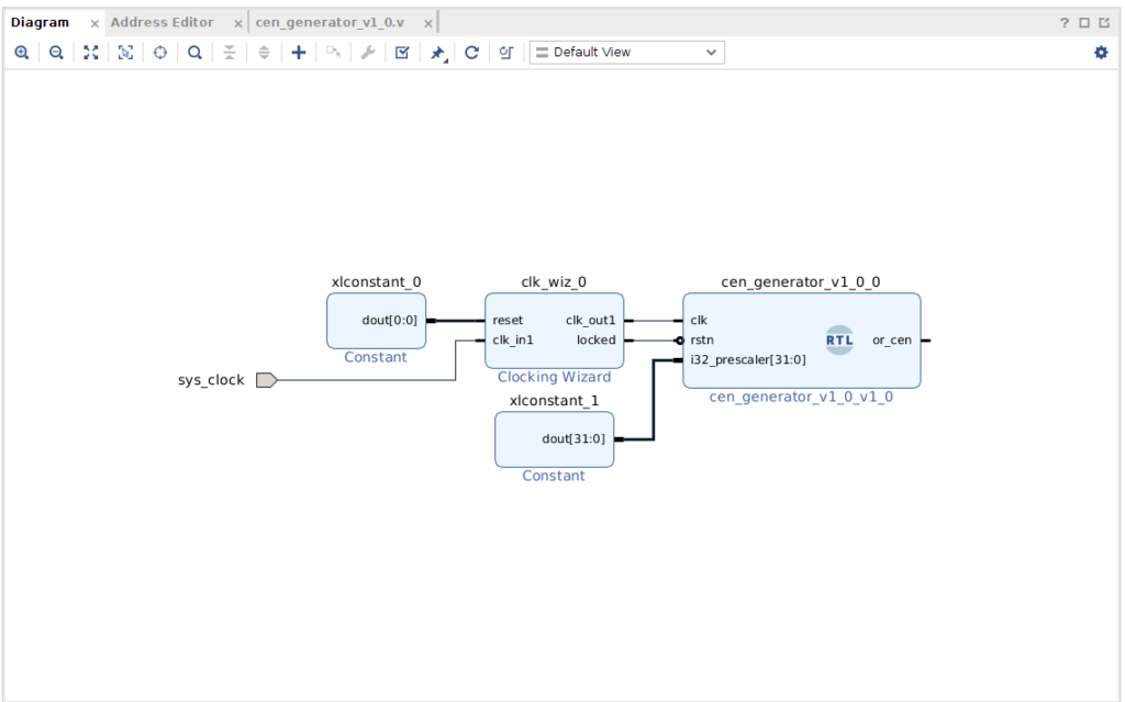
The next module we will add is the clock enable generator (cen_generator_v1_0). This block will generate a pulse for every ‘x’ clock cycle. The value of ‘x’ will be configured externally with a constant value. To add this block, we have to add a module, and then select cen_generator_v1_0.
As this module uses an inverted reset, we can use the locked output of the Clocking Wizard as reset.
/**
  Module name:  cen_generator_v1_0
  Author: P Trujillo (pablo@controlpaths.com)
  Date: Mar20
  Description: Clock enable generation according prescaler input.
  Revision: 1.0: Module created.
**/

module cen_generator_v1_0 (
  input clk,
  input rstn,

  input [31:0] i32_prescaler,
  output reg or_cen
);

  reg [31:0] r32_prescaler_counter;

  always @(posedge clk)
    if (!rstn) begin
      r32_prescaler_counter <= 32'd0;
      or_cen <= 1'b0;
    end
    else
      if (r32_prescaler_counter >= i32_prescaler) begin
        r32_prescaler_counter <= 32'd0;
        or_cen <= 1'b1;
      end
      else begin
        r32_prescaler_counter <= r32_prescaler_counter + 32'd1;
        or_cen <= 1'b0;
      end

endmodule
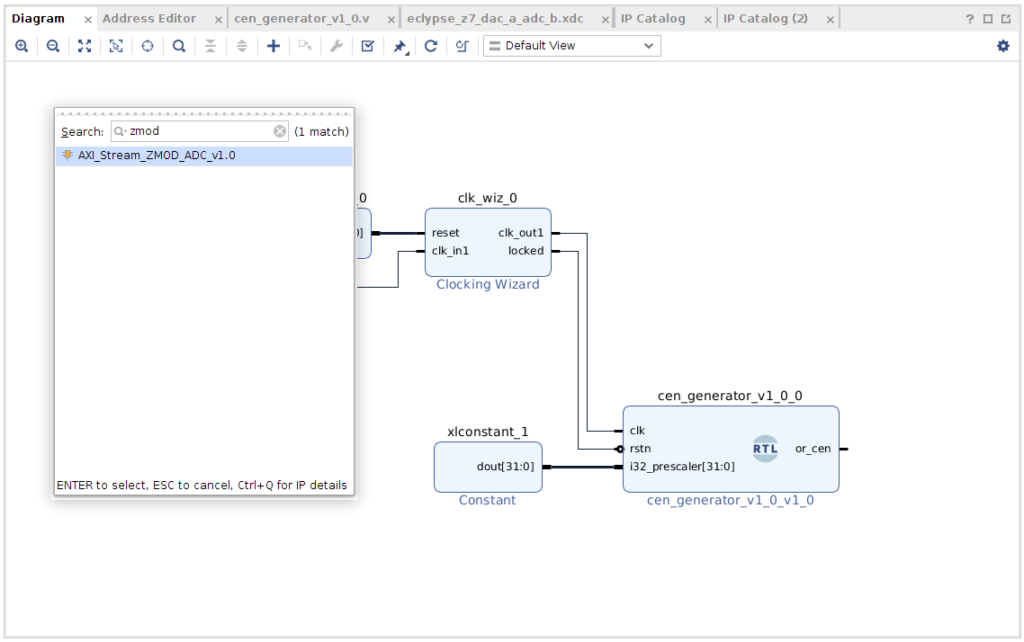
The next module we will add is the ADC driver. For this application, we will use the AXI (Advanced eXtensible Interface)-Stream Interface IP.
Once the IP is added, we need to generate all the ports, and to connect clock and reset.
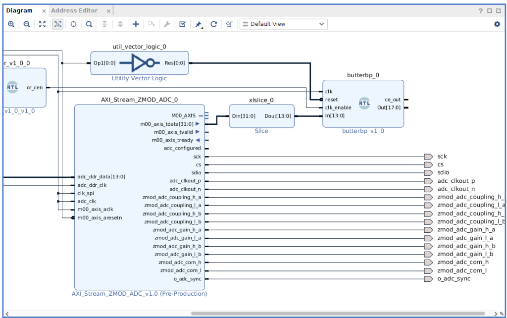
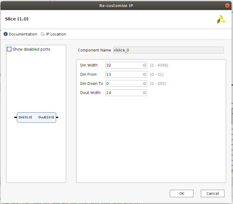
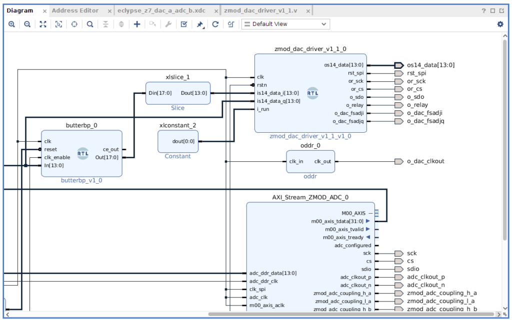
The next block we will add is the filter itself. When connecting this block, we have to take care because the output of the AXI Stream IP is 32 bits wide, and it contains the data from both ADC channels. Data corresponding to channel 1 is located on the 14 LSB.
To use only the lower 14 bits, we need to add a Slice block configured as shown in the figure following.
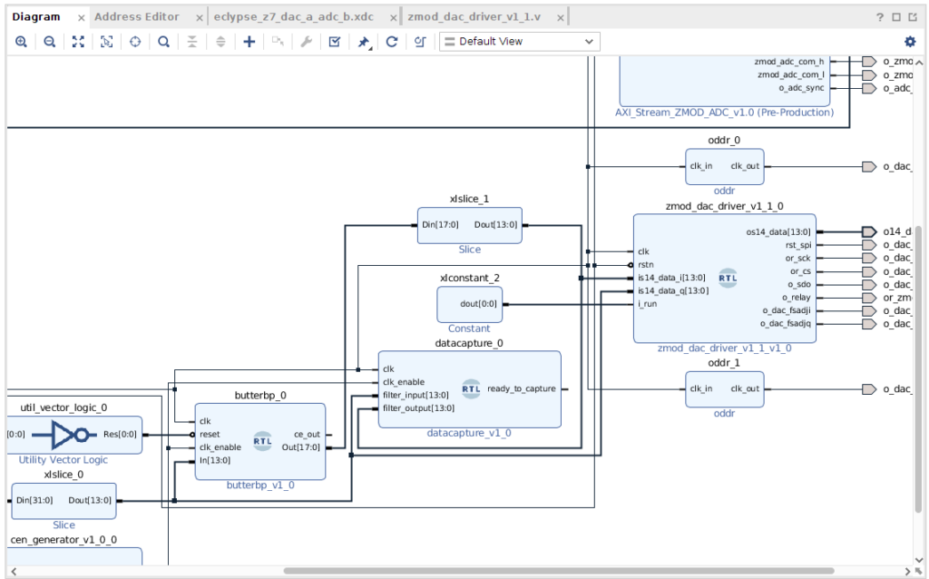
Also, the reset of the filter is active high, so we need to invert the reset of the rest of the design. Last, the clock enable line will be connected to the clock enable generator.
The last block we need to add is the DAC Driver. As the filter output is 18 bits wide, we need to discard the upper bits. Again, we will use a Slice block. We will connect the filtered output to the first channel of the DAC and the original signal to the second channel. This way, we can verify the effect of the filter on an oscilloscope. Notice that clock to the DAC has to be generated through an ODDR block.
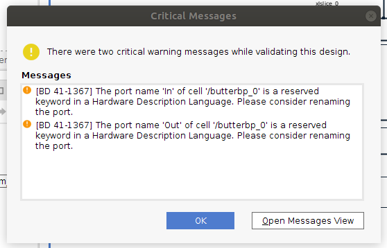
Once the block design is complete, we can validate the design. The result of the validation will be 2 warnings that ask us to change the input and the output port of the filter. In our case, we can ignore these warnings.
Next, we have to generate the HDL Wrapper by clicking on Generate Bitstream.
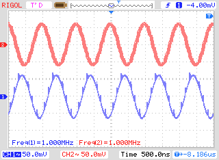
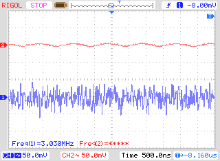
Once the design is synthesized and implemented, we can test our application on the Eclypse Z7 board with the Zmod Scope and the Zmod AWG attached to it, a signal generator, and an oscilloscope. First, we will set the signal generator to generate a 1MHz sine signal, with the result shown in the figure following (Ch1: input signal, Ch2: output signal).
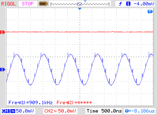
Now we check stopband. For this, we have to generate a 910kHz signal. At this input frequency, the output signal will have –60dB of gain, which is almost 0.
Using an oscilloscope is a good choice to test the filter, but in most cases, only the visualization of the signal won’t give us all the information we need to verify the filter. A good option could be to insert an Integrated Logic Analyzer (ILA) from Xilinx, to acquire the input and output data, and to export them to MATLAB. But MATLAB has a tool to do that directly: Data Capture. This tool captures data directly to MATLAB by adding an auto-generated IP and transfers the data to MATLAB through the JTAG port.
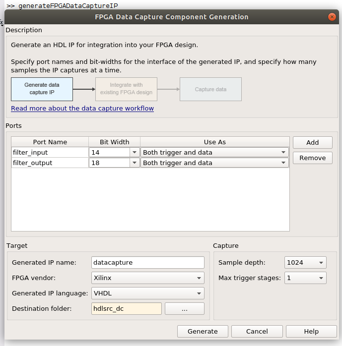
First, we need to generate the IP core for the data acquisition. In the MATLAB workspace, we will execute the command generateFPGADataCaptureIP.
In the window showing, we have to configure the tool. For our example, we will add 2 ports to capture the filter input and output, and we can select the sample depth for the number of samples captured for each port.
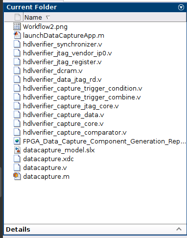
Then, by clicking on Generate, a module datacapture.v will be created in a folder of our choice. Also, a script launchDataCaptureApp.m will be generated to start the data capturing from MATLAB workspace. A Simulink model named datacapture_model.slx is also generated to capture data from Simulink.
Now, we have to add all .v files (.vhd in case of select vhdl) to the project. It is important to add all files because the datacapture module instantiates all these files.
Once we have added all these files to the design, we have to add the datacapture module to the block design and to connect all the ports.
Finally, click on Generate Bitstream and wait.
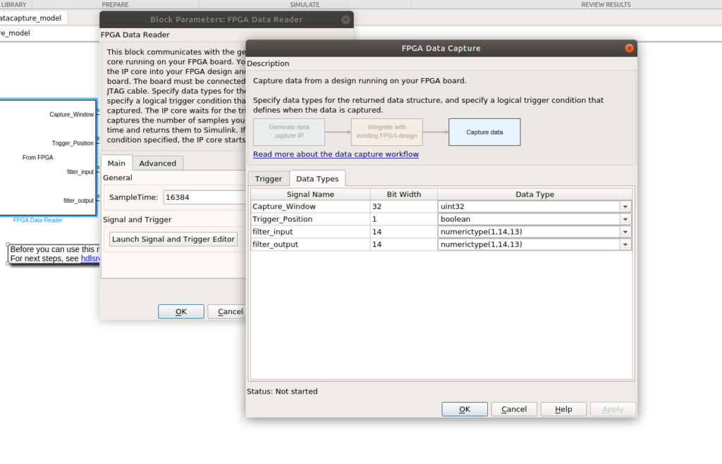
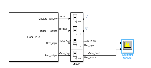
Once we have the design running on the FPGA, we have to close the hardware server from Vivado to release the JTAG port. Now we will open the Simulink model datacapture_model.slx, and we will make some changes. First, we will delete the scope. Then, we must configure the data format. To do that, we will click on the From FPGA block, and we will open the Signal and Trigger editor.
In this window, we will change the data type of the filter input and output data to numerictype(1,14,13), that means a signed number of width 14 with 13 bits of fractional part. Once we have this configuration done, we will change the input wave generated by the signal generator to a white noise wave. At this point, we cannot see information about the behavior of the filter on the oscilloscope.
To have a closer look at the signal, we will add a spectrum analyzer to our Simulink model.
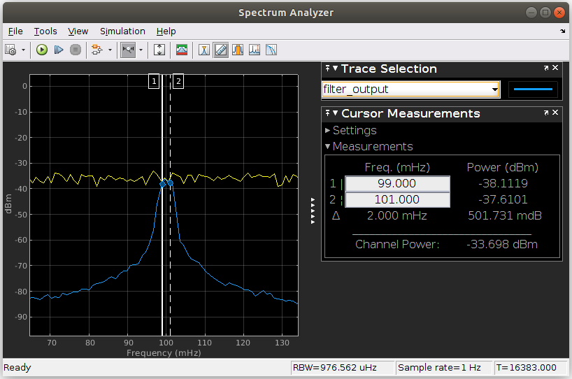
The white noise generated by the signal generator contains all the harmonics. If we filter a white noise signal, the output of the filter corresponds to the Bode diagram of the filter. And this is exactly what happened in our design.
In the figure above, we can see that the filter works without attenuation in the range from 990kHz to 1010kHz (notice that the sample rate for the analyzer is 1Hz, instead of 10MHz of the real design).
During this project, we have designed a filter with MATLAB, and we have followed a complete workflow from the theoretical filter design to the implementation of a real design and have verified the actual behavior of the filter. It is very interesting to see how MATLAB is integrated into the FPGA design workflow and how the tools make the development and test of such applications easy.


