Implementing a DC remover filter on FPGA
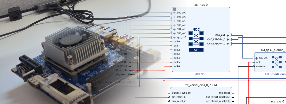
 Eclypse Z7
Many digital signal processing systems like audio processors or QAM decoders need at their input an AC signal and just an AC signal. The presence of a DC component, or DC bias in the input signal can make our system saturate or generate some type of missfunction. To avoid the DC bias in the output, a series capacitor can fix some cases but, what happens if the signal is already inside our system? In this case, we need a digital algorithm capable of removing the DC component of a signal affecting the less as possible to the AC component. The first solution that comes to our engineer’s minds is high-pass filters, but in general, they have a large transition band that, in many cases, is undesirable. Is true that we can use higher-order filters that reduce the transition band but, what about having a very narrow transition band using a first-order filter? This is exactly what we obtain using the next transfer function.
\[h(z)=\frac{1-z^{-1}}{1-\alpha z^{-1}}\] \[\alpha \exists[0,1]\]First, we are going to simulate the behavior of the filter in MATLAB. In the script, first, we have to declare the z variable, and then build the hz function. For the first this example we will use an alpha value of 0.95.
fs = 10e6;
ts = 1/fs;

z = tf('z', ts);

% filter declaration
alpha = 0.95;

hz = (1-z^(-1))/(1-alpha*z^(-1));
[num, den] = tfdata(hz);

freqz(num{1}, den{1})
The freqz function returns us the frequency response of the filter. We can see that the filter is indeed a high-pass filter but, unlike a first-order high-pass filter, the stop band of this filter is very narrow. We can control how narrow the stop band is by changing the value of alpha but remember that this value is the position of the pole, so making this closest to one can make the filter unstable due to quantization error in the fixed-point version of the filter.

")
Now, we can test the filter response by creating a sine signal and adding to it a step that will represent an offset change. The signal I generated is a 300kHz signal with three different levels of offset, first a null offset, a high offset of the 80% of the amplitude, and finally a small offset of 10% of the amplitude.
% signal generation
t = 0:ts:0.0001;
f = 300e3;

signal = sin(2*pi*f*t);
offset = [zeros(1,floor(length(t)/3)), 0.8*ones(1,floor(length(t)/3)+1), 0.1*ones(1,floor(length(t)/3)+1)];

signal_offset = signal + offset;

figure
plot(t,signal_offset);
grid minor

% filter signal
signal_filtered = filter(num{1}, den{1}, signal_offset);
The response of the filter is shown in the next figure.

Now, we are going to translate the filter transfer function into a block diagram. To do this, first, we need to obtain the equation of the filter.
\[\frac{y(z)}{x(z)}=\frac{1-z^{-1}}{1-\alpha z^{-1}}\] \[y(k)-y(k-1)\alpha=x(k)-x(k-1)\] \[y(k)=x(k)-x(k-1)+y(k-1)\alpha\]Using this equation we can deduce how this filter works. The term \(y(k)=x(k)-x(k-1)\) is a first-order high-pass filter. The frequency response of this filter has a large stop band with the typical 20dB/dec rise ramp. To make the stop-band narrower, the filter uses the term \(y(k)=x(k)+y(k-1)\alpha\), which is an integrator. This term compensates the gain in the stop band but also reduces the attenuation in DC.
Increasing the value of alpha will increase also the gain compensation, but the response time of the filter will be higher. In contrast, reducing the value of alpha will make the filter faster, but its response will be getting closer to the first-order filter.
The diagram of the filter is the one you can see in the next figure.

If you are familiar with control engineering, you will notice that this diagram can be simplified by swapping both loops. We can di this because they are in series.

Now, we can mix both delays into just one, so the new diagram will be the next.

Making this, which at a glance makes the diagram simplest, has a big problem when we implement it in fixed-point. To find it out, we are going to implement both diagrams using Simulink.

Now, we can check that the output of both diagrams is the same.

At this point, we are sure that the response is the same, so the filter is equivalent. Now, let’s take a look at the internal signals of the diagram. I have named the paths of the reduced diagram as upper_path and lower_path. Now, we can plot them and we can see that their values are quite higher than the input and output signals, which have an amplitude of one.

This means that, in the fixed point version of the filter, the width of the internal signals has to be quite larger than the input and output signals. In addition, how much these signals grow depends on the alpha value, which can be controlled, and the DC value, which is completely external.
For the “big” version of the diagram, we have the path mid_path, which is the output of the high-pass filter, so the max value that it will take will be the input signal, in case the input signal is in the pass-band. In the next waveform, we can see that the sine signals is not in the pass-band so it gain is around 0.2, and then we have a spike due to the offset change.

Now it’s FPGA time. The implementation of this filter in Verilog is quite simple. We have to obtain the delayed versions of the input (i_data_internal_1), and the output (o_data_internal_1) signals, and then multiply the delayed version of the output signal by the alpha input. First, all the signals are resized to internal_width to increase the resolution of the internal operations.
module dc_remover_v1_0 #(
  parameter inout_width = 16,
  parameter inout_decimal_width = 15,
  parameter internal_width = 24,
  parameter internal_decimal_width = 22
)(
  input wire aclk,
  input wire resetn,

  input wire signed [inout_width-1:0] alpha, /* filter alpha parameter */

  input wire signed [inout_width-1:0] i_data, /* input data */
  input wire i_data_valid, /* input data valid */

  output wire signed [inout_width-1:0] o_data, /* output data */
  output reg o_data_valid /* output data is ready */
);

  localparam inout_integer_width = inout_width - inout_decimal_width;
  localparam internal_integer_width = internal_width - internal_decimal_width;

  wire signed [internal_width-1:0] i_data_internal; /* input data resized to internal width */
  reg signed [internal_width-1:0] i_data_internal_1; /* input data k-1 */
  wire signed [internal_width-1:0] o_data_internal; /* output data resized to internal width */
  reg signed [internal_width-1:0] o_data_internal_1; /* output data k-1 */
  wire signed [internal_width-1:0] alpha_internal; /* alpha parameter resized to internal width */

  wire signed [(2*internal_width)-1:0] o_data_internal_1_alpha; /* output data k-1 times alpha */
  wire signed [internal_width-1:0] o_data_internal_1_alpha_resized; /* output data k-1 times alpha resized */

  /* resize input data to internal width */
  assign i_data_internal = $signed({ {(internal_integer_width-inout_integer_width){i_data[inout_width-1]}}, i_data, {(internal_decimal_width-inout_decimal_width){1'b0}}});
  assign alpha_internal = $signed({ {(internal_integer_width-inout_integer_width){alpha[inout_width-1]}}, alpha, {(internal_decimal_width-inout_decimal_width){1'b0}}});

  /* registers */
  always @(posedge aclk)
    if (!resetn) begin
      i_data_internal_1 <= 0;
      o_data_internal_1 <= 0;
    end
    else
      if (i_data_valid) begin
        i_data_internal_1 <= i_data_internal;
        o_data_internal_1 <= o_data_internal;
      end

  /* apply alpha gain */
  assign o_data_internal_1_alpha = alpha_internal * o_data_internal_1;
  assign o_data_internal_1_alpha_resized = $signed(o_data_internal_1_alpha >>> internal_decimal_width);

  assign o_data_internal = o_data_internal_1_alpha_resized + i_data_internal - i_data_internal_1;

  /* output data resize */
  assign o_data = o_data_internal >>> (internal_decimal_width-inout_decimal_width);

endmodule
At this point, I simulate the algorithm with a sine signal that changes its offset. The results of the simulation are the next.


We can see that the response of the implemented filter is quite similar to the simulated on MATLAB.
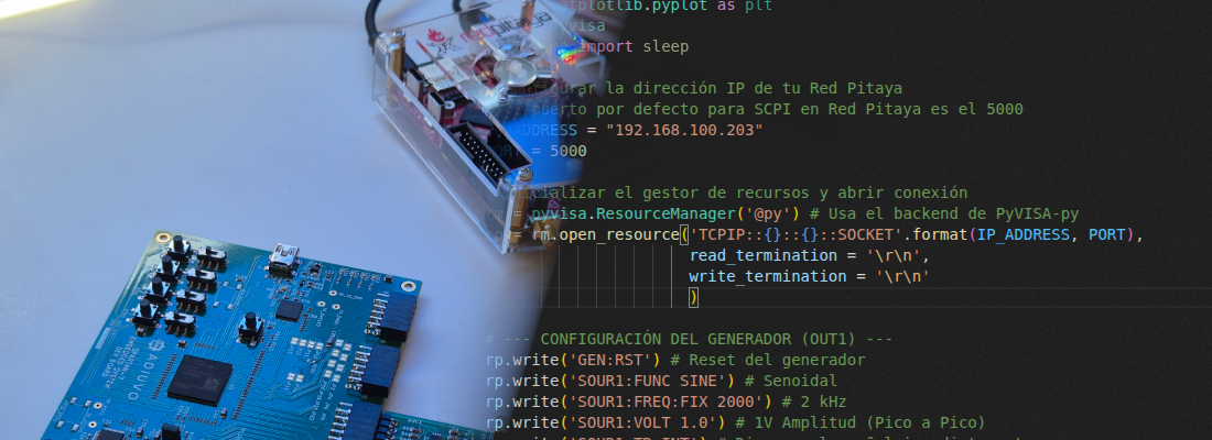
Finally comes the most interesting part, the verification on the FPGA. For this project I have used the Eclypse Z7 board, with the ZMOD DAC, now ZMOD AWG, and the ZMOD ADC, now ZMOD Scope. The signal is acquired by the ADC at 100 Msps. Since the simulation I did was with a sampling frequency of 10 Msps, I have decimated the input data rate to 10 Msps, then the signal arrives to the filter. The output of the filter is sent to the DAC where, again, the signal in sampled at 100 Msps. Both for the signal generation and the oscilloscope I used the ADC5250 from Digilent.

In the next figures, the blue signal is the input signal while the red one is the output signal. I have executed different offset steps over the 300 kHz AC signal.


DC signals on AC algorithms like audio processing can produce some undesirable effects like saturation or distortion. The DC bias can be removed indeed by hw, by placing a capacitor in series with the input ADC but, what happens with the DC bias of the ADC? In this case, the enemy is inside our system so, in these cases, a digital algorithm to remove it is very useful. The option I have presented you is not the only one, some other algorithms can remove the DC bias, but this one is perfect when you need to remove the DC bias in real-time without affecting so much the AC signal.