Implementing and ADC inside the FPGA
In my job, and also in the blog, I used to work with hardware-in-the-loop (HIL) systems. These devices can simulate in real-time the behavior of different analog circuits, and allow us to design algorithms and electronic circuits to control those circuits and test them against that real-time simulation of the circuit. These devices are very common when we are designing power converters, and want to test different control algorithms, actually, in this blog we can find different articles that use the Speedgoat real-time target machine (/2024/02/04/subcycle-average-part-1/). For a complete simulation of the circuit, ideally, we are going to use our electronic boards. This way we can test both the algorithm and the electronics but, what if we don’t have the electronic board yet? In some cases, especially in the early stages of development, we usually develop the algorithms using some development boards from the controller manufacturer, so it will be quite common that PWM drivers or analog to digital converters (ADC) are not available on those development boards. PWM drivers won’t be a problem because of the wide range of the HIL digital inputs, but ADCs are something that will be necessary. HIL devices have analog outputs ready to be connected to our electronic board, so in principle, there is no choice, we need ADCs, or not?
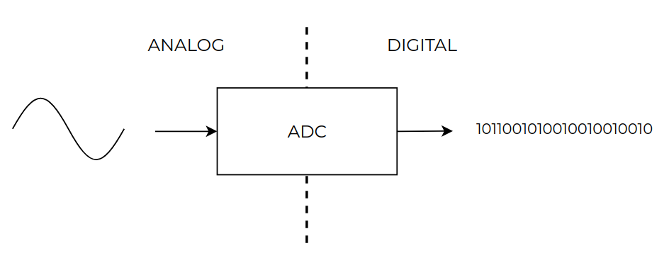
Let’s start from the beginning, what is an ADC? An ADC is an integrated circuit with an input and an output. In the input and the ADC we are going to connect an analog signal, for example, the current through an inductor if we are controlling a power converter, and even just a voltage that depends on the ambient temperature measured by an NTC. The output of an ADC will be a digital signal that represents the value of the input analog voltage. For example, if we have a 10-bit ADC, the input analog voltage will be translated into a value in the range 0-1024. The time spent by the ADC to convert each sample is the sampling period of the converter. How the digital data is sent to the controller can be parallel, an SPI protocol, I2C, \(\delta \sigma\) modulation… A (very) simplified diagram of an ADC would be the next.
Now that we know what is an ADC, let’s connect it to a HIL device. As I mentioned before, HIL devices use digital-to-analog converters (DAC) to convert the digital data from the FPGA to an analog signal that will be read from our electronics board. So, by adding the ADC to the last diagram, we will have this.
This converters party makes sense when (1) the ADC acquisition is ready, and/or (2) the ADC acquisition is very relevant. For (1) is very clear, if we don’t have the electronics board manufactured, or the project is just a probe of concept so we are not going to spend money manufacturing a custom board, and we just going to use development boards, the converters party makes no sense. For (2), it could be a reason to discuss. When the ADC acquisition is relevant? Always. End of discussion? not really. If we consider that, in this case, we are simulating an entire analog circuit using FPGA, and we are going to take the simulated behavior as good enough, why not do the same with the ADC? Why not integrate the ADC in our model and eliminate the DAC outputs, and also the need for ADCs in our electronic circuits? This is exactly what is a virtual ADC (vADC).
A vADC is an FPGA IP that acts as an ADC and can integrate different interfaces to send the digital data to the controller. For example, if we are developing an electronics board that features a TI ADC122S101, the v_ADC122S101 will be based on an SPI slave that sends the read analog voltage codified in 12 bits. The same IP we use for the ADC122S101 will be valid for the ADC122S021 and the ADC122S051, since the only difference between them is the acquisition time.
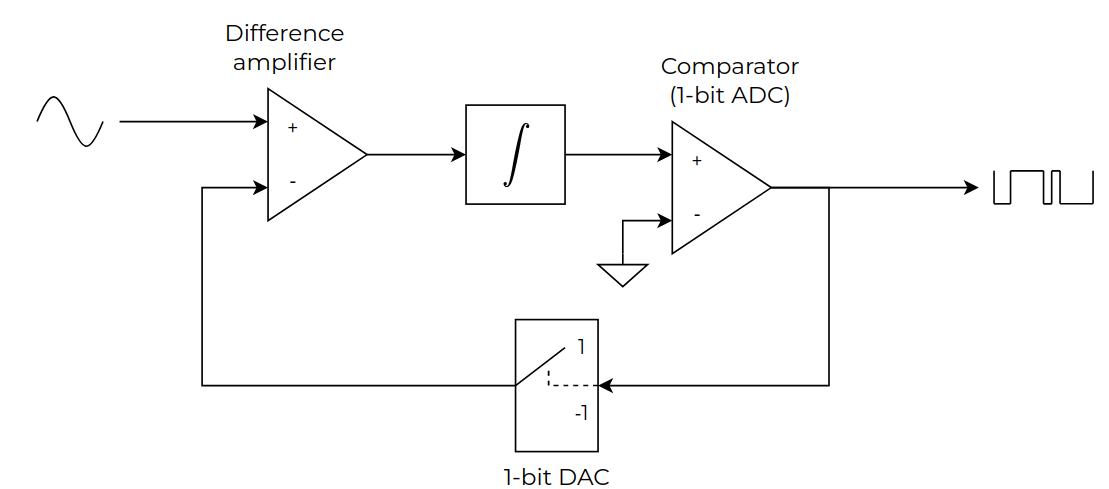
An ADC topology widely used in power converters are \(\delta \sigma\) (delta-sigma) modulators. This type of ADC converts the analog input voltage into pulse-density modulation (PDM). The structure of these modulators is shown in the next figure.
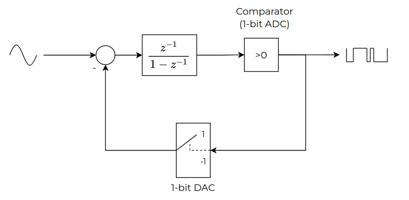
If you are familiar with digital signal processing, you will notice that this structure is easy to discretize. In the next figure you will find the delta-sigma structure but translated to the FPGA language.
Implementing this on an FPGA is as easy as the next snippet.
/* pipeline */
always @(posedge aclk)
	if (!resetn) begin
		input_data_diff_1 <= {DATA_WIDTH{1'b0}};
		output_integrator_1 <= {DATA_WIDTH{1'b0}};
	end
	else
		if (ce) begin
			input_data_diff_1 <= input_data_diff;
			output_integrator_1 <= output_integrator;
	end

/* input diff */
assign input_data_diff = input_data - output_data_quantized;

/* integrator */
assign output_integrator = {input_data_diff_1[DATA_WIDTH-1], input_data_diff_1} + {output_data_1[DATA_WIDTH-1], output_data_1};

/* output comparator */
assign output_data = (output_integrator[DATA_WIDTH])? 1'b0: 1'b1;

/* 1-bit dat */
assign output_data_quantized = (output_data)? {1'b0, { {DATA_WIDTH-1}1'b1}}: {1'b1, { {DATA_WIDTH-1}1'b0}};
Notice that the integrator uses the last input, not the actual one, This is because if we use the newer one, in the circuit appears an algebraic loop that needs to be broken adding a delay, that in this design is already added in the integrator.
This kind of modulator works at frequencies of several megahertz, being 10 Mhz is quite common. The key of these modulators is that the modulator and demodulator go together, and according to the features of both we will obtain the effective number of bits and the sampling rate. The best is that both the modulator and the demodulator can be implemented on FPGA so, who need ADCs?
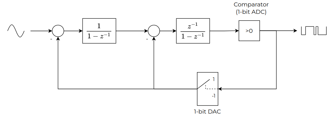
I realized that delta-sigma modulators/demodulators deserve an entire article talking about them, so for now, an extra feature that you need to know is that, although the modulator is like a 1-bit DAC, due to its structure they attenuate the noise in the base-band, so the signal of interest is quite clean. If we need to improve the attenuation, you can implement a higher order modulator. In the next figure you can find a second-order delta-sigma modulator.
Virtual ADCs are an essential part of a project that will be presented soon here, and it is very related to HIL devices. Are vADC valid for all the projects? No, it depends on the application and, especially, if there is a vADC IP of your ADC. Also, if you have an electronic board already manufactured, with all your ADCs, vADC is not for that project, on the other side, if you have an idea, and just have an FPGA board, yes, it could be very useful for you.


