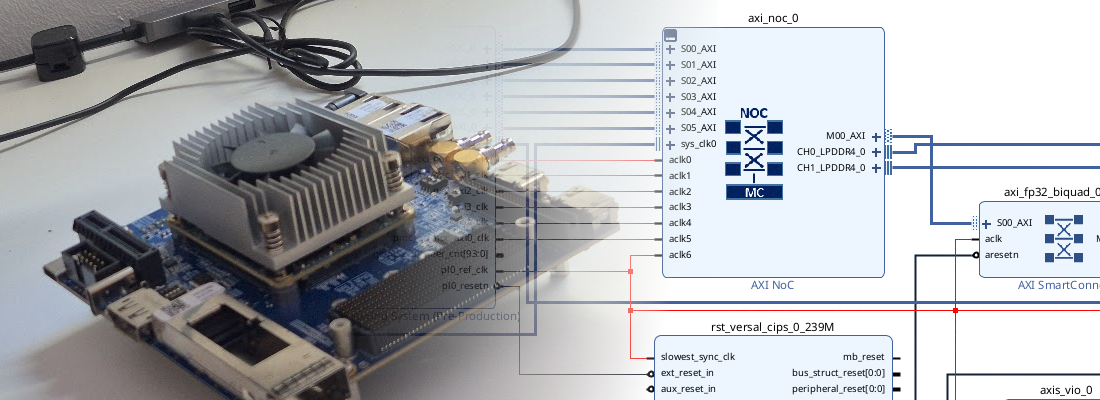
Solving a Boost converter in FPGA
A few weeks ago I read an article that talked about how to solve differential equations on FPGA. That article was very interesting but then I realized that it is not a complex task for FPGA as long as the equation could be discretized. The problem comes when you mix ODE with piecewise linear systems, where the behavior of the systems depends on the state of a variable that changes in a non-linear way. Despite this, implementing an ODE solver in FPGA is something that we already did in this blog so, can we go further? yes, how about using the FPGA to solve electrical circuits? in this case we are going to implement a Boost power converter in the FPGA.
The static transfer function of a Boost converter is the next.
\[v_O = VDC \frac{1}{1-D}\]We can see that for \(D=0\), the output voltage is the input voltage, and then while the duty cycle increases, the output voltage does the same.
In the next figure, you will find the electric schematic of a Boost converter. This converter has many differences from the Buck converter modeled here. From a mathematical point of view, we can see that the switch is in the middle between the inductor and the output, so it cannot be modeled as a pulse train between zero and VCC. Also, when the switch is activated, the inductor is connected to the ground, which is the opposite behavior we saw in the buck converter.

To start modeling the converter we need to identify the different variables we have. By solving these variables we will be able to solve the circuit for any value of \(t\). The variables are almost the same as we can find in any converter.

First of all, we have the current through the inductor, which follows the next equation
\[i_L(t) = \frac{1}{L} \int v_L(t) dt\]Then we have the voltage of the capacitor which is the same as the output voltage, and follows the next equation
\[v_C(t) = \frac{1}{C} \int i_C(t) dt\]These two equations can be discretized using either the Impulse Invariance method or Tustin. In this case, I used the Impulse Invariance because it is easy to implement, but both of them would have similar behavior.
\[H(z)=\frac{T}{1-z^ {-1}}\]Finally, we have the equation of the resistor current
\[i_R(t) = \frac{v_C(t)}{R}\]If we want to improve the confidence of the model, in boost converters there is another variable that limits the output voltage of the converter, the inductor’s resistor. Let me explain this. Boost converters, like everything, meet the thermodynamics rules, that is, the output power will be always less than the input power. Therefore, since the boost converter elevates the input voltage, it needs to increase the input current proportionally so, if we want to double the input voltage in the output, the input current will be twice the output current, and all of this current flows through the inductor. If the inductor has no resistance, this relation can be extended until \(D=1\) with an output voltage of infinite volts. Adding this resistor, in this case, the voltage in the ideal inductor is reduced while the input current is increased, reaching a limit in the output voltage. The equation of this resistor is quite simple. The current across this resistor is the same as the inductor current, so we can calculate the voltage loss as follows.
\[v_{RL} = i_L(t) \cdot RL\]Now it’s time to join all the equations, and here we will find the main difference between the Boost and the Buck converter. In the Buck converter, the only variable that changes with the switching is the input voltage. In this case, we can find that the current that flows through S2 depends on the state of S1, being 0 when S1 is active. This is because the diode just allows the current flow in one direction, so when v2 is connected to ground S2 behavior is like an open circuit, and \(i_C+i_R = 0\). Another variable that modifies its behavior with the switching is the inductor voltage, and therefore the inductor current. In the next figure, you will find the whole circuit we are going to model.

Translating the last paragraphs into equations, we will have the next discontinuities.
The capacitor and the resistor current change with the switching, and its behavior would be the next.
\[i_C+i_R = \Bigg \{ \begin{matrix} 0 & S1 = ON\\i_L & S1 = OFF \end{matrix}\]Then, the inductor voltage can be calculated as
\[v_L = v1 - v2\]From these two variables, \(v1\) is always connected to VDC, but \(v2\) depends on the switching state.
\[v2 = \Bigg \{ \begin{matrix}0 & S1 = ON\\v_C & S1 = OFF \end{matrix}\]Adding the inductor’s resistor, its voltage depends on the current that flows through it.
\[v1 = VDC - i_L \cdot R_L\]Now we can translate these equations into a Simulink circuit.

In the Simulink circuit, you can see all the variables calculated with blocks and discrete integrators. If we simulate this, Simulink will return a warning that indicates the presence of algebraic loops in the circuit. An algebraic loop means that to obtain the value of a variable, we need to know the value of that variable. In the circuit, we have two algebraic loops, one in the \(i_L\) calculation
\[i_L(t) = \frac{1}{L} \int v_L(t) dt = \frac{1}{L} \int v1(t)-v2(t) dt = \frac{1}{L} \int (vdc-i_L(t)\cdot RL) - v_C(t) dt\]and the other one in the capacitor voltage
\[v_C(t) = \frac{1}{C} \int i_C(t) dt = \frac{1}{C} \int i_L(t)-i_R(t) = \frac{1}{C} \int i_L(t)-\frac{v_C(t)}{R}\]Mathematically this is solved by setting an initial condition in those variables. Talking FPGA, that means that we need to initialize those variables, in other words, we need to register the variables and set a value for the reset but notice that the delays included to break the algebraic loops work at different periods than the delays of the integrators.
For the integrators, we need to integrate at the sample time in which the model will be calculated, in this case, \(1us\).

On the other side, the delays added in the algebraic loops have to run at the clock speed. If we run these delays at the sampling time, the behavior of the model will change completely, but adding delays with the fastest clock just means a delay in the output of a clock period. For this Simulink model, I have set the solver time step at 100ns.

Therefore the delays for the algebraic loops can be configured with a sample time of -1, and they will take the maximum speed of the model, which is the solver time step.

In the Verilog code that simulates this circuit, the switches are modeled like the next code. Notice that this switch must be registered since it is an external signal, and although I have not used a synchronizer (set of two registers in series) to read the input, it is important to, at least, register the input signal.
/* current through the capacitor + resistor */
always @(posedge aclk)
  if (!resetn)
    iCR <= {data_width{1'b0}};
  else
    iCR <= S1_pwm? {data_width{1'b0}}: iL;
Here you can find how the registers added to break the algebraic loops work at clock frequency, with no clock enable or data valid signal.
/* capacitor current */
always @(posedge aclk)
  if (!resetn)
    iC <= {data_width{1'b0}};
  else
    iC <= iCR - iLoad;
Finally, here you can find the integrators. In this case, the integration is performed at the sampling frequency, so the register works just with the ce (clock enable) signal.
/* inductor current integrator */
assign iL = vL_k + iL_1;

always @(posedge aclk)
  if (!resetn)
    iL_1 <= {data_width{1'b0}};
  else
    if (ce)
      iL_1 <= iL;
The rest of the code are additions and shifts.
I have performed some simulations of this model and all of them went pretty well. The next simulation shows the response of the system when the load resistor decreases its value. The conditions of this test were
- VDC = 100 Volts
- PWM = 50%
- L = 100uH
- C = 330 uF
- R = 10 -> 1 ohms
We can see how the system oscillates and the iLoad doubles its value. The output voltage before the event was 200 volts with a minimum ripple. Then, after the event the ripple is increased. This is because when the switch is activated, the Capacitor discharges its energy to the resistor, so as a high current demands the load, more will be the voltage fall of the capacitor. In addition, the average value of \(v_C\) has decreased due to the inductor resistor.

As I said before, solving this kind of electrical circuit is “just” solving differential equations on FPGA. Doing some tests, I have realized that the Simulink simulations take several seconds to simulate 500ms, while the FPGA can run this model in real-time, so we can see this project as a kind of accelerator to solve ODEs. To do this we just need to translate the circuit into a synthesizable code and execute it on FPGA.
The code of this model will be available in a few weeks. The reason is that this model is part of another project I have been developing for some weeks, and it will be presented soon.