Implementing a FIR filter using folding.
In this blog we have seen how to develop an FIR filter. In this post you have an example of FIR filter where the coefficients are configured through AXI4-Lite interface. The goal of that post was the implementation of a configurable digital signal processing algorithm on the edge, without focusing on the FIR implementation. On this post, we will see how the synthesizer reads the Verilog code, and converts this lines to a digital circuit. Although my idea in this post, is not focusing on the FIR filter design, we need to know what is an FIR filter before understand its implementation.
FIR filters are a pure digital filter implementation. Unlike the IIR filters, where the design starts with a continuous filter design, and then this filter is discretized, FIR filters are designed digitally from the beginning. The transfer function of a 4th order FIR filter is the next.
\[h(z)=b0 + b1 \cdot z^{-1} + b2 \cdot z^{-2} + b3 \cdot z^{-3} + b4 \cdot z^{-4}\]You will notice that the transfer function has only the numerator. It means that in this kind of filters, there are no poles. In other words, the response of the FIR filters only depends on the input now, and the input before. That is the reason this kind of filter is also known as all zeros filters, and this has a great advantage over the IIR filters, FIR filters are always stable. On the other hand, the fact that the output only depends on the input makes the response of this filter softer than the IIR filters, and this means that for a response equivalent to an IIR filter, the order must be much higher. In the next diagram, you can see the map of poles and zeros of an FIR filter.
According to the transfer function, we only need to perform multiplications and addition to implement an FIR filter, and that is well new, because the DSP48 Slices for Xilinx devices, and MACC blocks for Microchip devices, are designed to perform this operation. As I did with the biquad filter, I will show and explain the code to implement, in this case, an 8th order FIR filter.
First, as we need a filter where the input and outputs width will be configurable, we have to define some parameters. Also, we will need to define the internal width to have the possibility to improve the resolution of the internal operations.
module axis_fir_8_v1_0 #(
  parameter inout_width = 16,
  parameter inout_decimal_width = 15,
  parameter coefficient_width = 16,
  parameter coefficient_decimal_width = 15,
  parameter internal_width = 16,
  parameter internal_decimal_width = 15
  )
Next we must define the interface of the module. For the input and output signals, I will use an AXI4-Stream interface. On the other hand, for the coefficients, I will use an RTL interface.
(
  input aclk,
  input resetn,

  /* slave axis interface */
  input [inout_width-1:0] s_axis_tdata,
  input s_axis_tlast,
  input s_axis_tvalid,
  output s_axis_tready,

  /* master axis interface */
  output [inout_width-1:0] m_axis_tdata,
  output reg m_axis_tlast,
  output reg m_axis_tvalid,
  input m_axis_tready,

  /* coefficients */
  input signed [coefficient_width-1:0] b0,
  input signed [coefficient_width-1:0] b1,
  input signed [coefficient_width-1:0] b2,
  input signed [coefficient_width-1:0] b3,
  input signed [coefficient_width-1:0] b4,
  input signed [coefficient_width-1:0] b5,
  input signed [coefficient_width-1:0] b6,
  input signed [coefficient_width-1:0] b7,
  input signed [coefficient_width-1:0] b8
  );
We have defined a width for the input and output signal, a width for the coefficients, and the width that the module will use internally, so the next thing we must do is to resize the input and the coefficients to the internal width, filling with zeros the decimal side, and with the MSB the integer side in order to keep the sign of the value.
/* resize signals to internal width */
assign input_int = { {(internal_integer_width-inout_integer_width){s_axis_tdata[inout_width-1]}},
                            s_axis_tdata,
                            {(internal_decimal_width-inout_decimal_width){1'b0}} };
assign b0_int = { {(internal_integer_width-coefficient_integer_width){b0[coefficient_width-1]}},
                            b0,
                            {(internal_decimal_width-coefficient_decimal_width){1'b0}} };
assign b1_int = { {(internal_integer_width-coefficient_integer_width){b1[coefficient_width-1]}},
                            b1,
                            {(internal_decimal_width-coefficient_decimal_width){1'b0}} };
assign b2_int = { {(internal_integer_width-coefficient_integer_width){b2[coefficient_width-1]}},
                            b2,
                            {(internal_decimal_width-coefficient_decimal_width){1'b0}} };
assign b3_int = { {(internal_integer_width-coefficient_integer_width){b3[coefficient_width-1]}},
                            b3,
                            {(internal_decimal_width-coefficient_decimal_width){1'b0}} };
assign b4_int = { {(internal_integer_width-coefficient_integer_width){b4[coefficient_width-1]}},
                            b4,
                            {(internal_decimal_width-coefficient_decimal_width){1'b0}} };
assign b5_int = { {(internal_integer_width-coefficient_integer_width){b5[coefficient_width-1]}},
                            b5,
                            {(internal_decimal_width-coefficient_decimal_width){1'b0}} };
assign b6_int = { {(internal_integer_width-coefficient_integer_width){b6[coefficient_width-1]}},
                            b6,
                            {(internal_decimal_width-coefficient_decimal_width){1'b0}} };
assign b7_int = { {(internal_integer_width-coefficient_integer_width){b7[coefficient_width-1]}},
                            b7,
                            {(internal_decimal_width-coefficient_decimal_width){1'b0}} };
assign b8_int = { {(internal_integer_width-coefficient_integer_width){b8[coefficient_width-1]}},
                            b8,
                            {(internal_decimal_width-coefficient_decimal_width){1'b0}} };
Once we have all the input to the module resized to the internal width, the next we will do is create the pipeline for the input signal. This will be done by using registers, and using the s_axis_tvalid signal as a clock enable.
/* pipeline registers */
always @(posedge aclk)
  if (!resetn) begin
    input_pipe0 <= 0;
    input_pipe1 <= 0;
    input_pipe2 <= 0;
    input_pipe3 <= 0;
    input_pipe4 <= 0;
    input_pipe5 <= 0;
    input_pipe6 <= 0;
    input_pipe7 <= 0;
    input_pipe8 <= 0;
  end
  else
    if (s_axis_tvalid) begin
      input_pipe0 <= input_int;
      input_pipe1 <= input_pipe0;
      input_pipe2 <= input_pipe1;
      input_pipe3 <= input_pipe2;
      input_pipe4 <= input_pipe3;
      input_pipe5 <= input_pipe4;
      input_pipe6 <= input_pipe5;
      input_pipe7 <= input_pipe6;
      input_pipe8 <= input_pipe7;
    end
Until this point, we have no many implementation options. Now we have to perform the MACC operations, and the way we implement this part, will produce differences in the resources used and the timing requirements. First, I have designed a parallel implementation with the MACC operation implemented without registers.
/* MACC structure */
assign input_b0 = input_pipe0 * b0_int;
assign input_b1 = (input_pipe1 * b1_int) + input_b0;
assign input_b2 = (input_pipe2 * b2_int) + input_b1;
assign input_b3 = (input_pipe3 * b3_int) + input_b2;
assign input_b4 = (input_pipe4 * b4_int) + input_b3;
assign input_b5 = (input_pipe5 * b5_int) + input_b4;
assign input_b6 = (input_pipe6 * b6_int) + input_b5;
assign input_b7 = (input_pipe7 * b7_int) + input_b6;
assign input_b8 = (input_pipe8 * b8_int) + input_b7;

assign output_int = input_b8 >>> (internal_decimal_width);
This implementation has advantages and disadvantages. First, you will notice that this design uses 9 DSP blocks. This could be a problem if we have a part where the DSP slices are limited. On the other side, the only logic we need are the registers, and the DSP blocks, so this implementation is very efficient in terms of logic. If we check the Vivado implementation, we can see clearly the nine DSP48E1 blocks, but we can see only six registers stages.
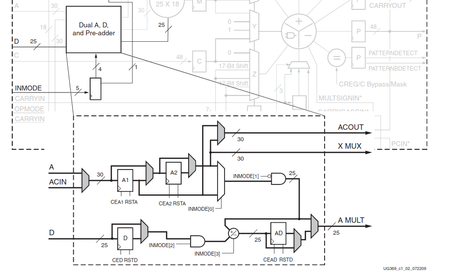
The other 2 register stages have been absorbed by the DSP Slices. If we check the DSP48E1 structure, we can find in the A input, registers A1 and A2, than can be bypassed by 2 multiplexers. In the case of the operation
assign input_b0 = input_pipe0 * b0_int;
Only one of these registers is used. For the second operation, both of these registers are used. That is the reason the input data is connected directly to the 2 first DSP48E1 Slices. For the third operation, as there are no more registers to use on the A input, the Synthesizer includes 1 set of registers out of the DSP Slice. For the rest of the multiplications, one register is added for each one.
In this case, the multiplication is done combinationally, that is, without a register on the output of the multiplier. This could cause that the timing requirement will be not met. To improve the speed of the design, we can add a register on the multiplication.
/* MACC structure registered */
always @(posedge aclk)
  if (!resetn) begin
    input_b0 <= 0;
    input_b1 <= 0;
    input_b2 <= 0;
    input_b3 <= 0;
    input_b4 <= 0;
    input_b5 <= 0;
    input_b6 <= 0;
    input_b7 <= 0;
    input_b8 <= 0;
  end
  else begin
    input_b0 <= input_pipe0 * b0_int;
    input_b1 <= (input_pipe1 * b1_int);
    input_b2 <= (input_pipe2 * b2_int);
    input_b3 <= (input_pipe3 * b3_int);
    input_b4 <= (input_pipe4 * b4_int);
    input_b5 <= (input_pipe5 * b5_int);
    input_b6 <= (input_pipe6 * b6_int);
    input_b7 <= (input_pipe7 * b7_int);
    input_b8 <= (input_pipe8 * b8_int);
  end

assign output_2int = input_b0 + input_b1 + input_b2 + input_b3 + input_b4 + input_b5 + input_b6 + input_b7 + input_b8;
assign output_int = output_2int >>> (internal_decimal_width);
The implementation of this code does not add logic to the design since this register is absorbed by the DSP48E1 Slice, by activating the MREG register. If this register will improve the timing or not will depend on the logic that we connect in the output of the DSP Slice.
Although these implementations are very easy, is possible that the use of nine DSP slices could be a problem. Even more, if we design a high-order FIR filter. In this case, we can use folding. Folding, in DSP, is a technique to share resources, by adding a delay. In other words, we can perform all the multiplications in parallel, using N+1 multipliers, or we can perform the multiplications in series, using only one multiplier. Also, we can design a mix of both, using more than one multiplier, and reducing the output delay. The relation between the number of multipliers used, and the number of multiplications to do is named as folding factor. For this example, I have designed the logic to implement folding with a folding factor of eight, that is using only one multiplier for the eight operations. Due to the logic I have designed, the total delay is ten clock cycles, but the design can be optimized to get a minimum delay of eight clock cycles.
/* one cycle delay */
  always @(posedge aclk)
    if (!resetn)
      s_axis_tvalid_1 <= 1'b0;
    else
      s_axis_tvalid_1 <= s_axis_tvalid;

  /* logic to perform macc operations */
  always @(posedge aclk)
    if (!resetn) begin
      index <= 3'd0;
      output_2int <= 0;
      output_int <= 0;
      m_axis_tvalid <= 1'b0;
      m_axis_tlast <= 1'b0;
    end
    else
      if (index == 9) begin
        output_int <= output_2int >>> (internal_decimal_width);
        output_2int <= 0;
        m_axis_tvalid <= 1'b1;
        m_axis_tlast <= m_axis_tlast_mem;
        index <= 0;
      end
      else if (s_axis_tvalid_1 || (index != 0)) begin
        index <= index + 1;
        output_2int <= output_2int + input_bn;
      end
      else begin
        m_axis_tvalid <= 1'b0;
        m_axis_tlast <= 1'b0;
        index <= 0;
      end

  /* macc operation */
  assign input_bn = input_pipe[index] * bx_int[index];
When we simulate both filters, we can see how in the serial implementation, each sample is delayed ten cycles. At this point, we have to answer ourselves if that delay is a problem. Well, for systems where the input signal has a sampling period greater than ten clock cycles, this filter is valid. In the case that the input signals have a period shorter than ten clock cycles, we will need to redesign our filter to be faster by adding another multiplier or increasing clock frequency.
We have talked about the implementation, but, what happens with the timing? Timing analysis in the case of an out-of-context module only can give us comparative information, because the place and route process when this module will be integrated with the rest of the design will be quite different, but we can extract some conclusions. The next table has been extracted for a 100MHz clock, and a XC7A200T piece.
We can see how the faster implementation is named as fir_reg, that is corresponding with the registered parallel implementation, but the gain in timing, with respect to the FF used, makes this implementation a little bit inefficient. In this case, in fir1 implementation, that is corresponding with the serial implementation, we can see how the DSP used is one, but the rest of the logic has been increased, and also the time needed. Finally the last implementation, fir_reg_retiming has been done enabling the retiming flag on the synthesizer for the fir_reg implementation, but there is no gain because the synthesizer has no logic to change.
We have seen 3 different implementations of the same FIR filter, and the use of one or another will depend entirely of the entire design. In the case that the part you are using has a limited number of DSP slices or MACC blocks, the use of the fir1 is highly recommended. Also, you can use this example to design a fir2, using 2 multipliers to increase the WNS, but I am not sure that the logic used decreases. In case you are using a big piece, o simply you do not need the multipliers for other parts of your design, the simplest, faster and most efficient way to design an FIR filter is the first.


