Designing an FPGA SOM.
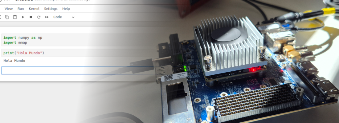
 CP SOM ONE
In the market we can find many different FPGA boards with infinite interfaces, peripherals, connectors… so anyone can think, why you would need to develop your own FPGA board. You just have to find a development board that meets most of your requirements, especially if you are a hobbyist and you just need one board. In addition, FPGAs are not cheap devices and on many occasions, it is cheaper to buy a development that features the FPGA you need, than buying the FPGA and then, developing your board. Well, all of these reasons are true, but, what about having your own FPGA board? An FPGA that meets all your requirements and also allows you to learn to develop a development board. In addition, if you have a blog to share the steps you followed, and can be used to help other FPGA developers, all the best.
How did this development start? well, the main reason to start this development is the next image.

The capture corresponds to JLCPCB Parts, the store of JLCPCB for its PCA service, and yes, you can find an Artix7 75t for just 30 dollars. The total cost of the assembly service will vary according to the complexity of your board, and the number of components… but in the end, you can have a development board with this FPGA for less than 250 dollars, actually I built three of them for this price. Let’s go to design the board!
First of all, a development board or a SOM? Well, I preferred to design a SOM because later, I can use it on different boards. Also, since the FPGA SOM is more complex than most applications where I need an FPGA, the cost of designing a carrier board may be ridiculous if I just use a two-layer board soldered by hand.
The FPGA I chose for the schematic is the xc7a35t with the package FGG484. Later, I used the xc7a75t. The reason for using the smallest device in the PCB design is that I want to be able to use all the FPGA that fits with this package. For the Artix7 FPGAs, although the packages are the same, bigger devices like the 75t of 100t have more IO banks than the 35t, so if I use the biggest device in the schematic I will have more IO available, so using one of these IO available just in the 75t or 100t, will make that the SOM with a 35T have some IO ports unconnected. The FPGA is included by default in the KiCad libraries, unlike the Spartan7 FPGA, so we just need to search it and add it to the schematic.
Then, we are going to design the power supply schema. All the AMD 7 series FPGAs use the same power supplies for the logic. If you want to use DDR RAM or the MGT, you will have to add some power supplies besides the ones I used in this design. In my case, I am going to use just the logic, so I need three voltages, 1.0 volts, 1.8 volts, and 3.3 volts. I used three TLV62565, a step-down converter with a maximum current of 1.5 Amps and a SOT23-5 package. This IC just needs an inductor, two capacitors, and two resistors to fix the output voltage.

The high number of capacitors on each converter output corresponds with the decoupling capacitors that need the FPGA. The amount of capacitors needed can be found in the UG483. In this document, in Table 2-2, you will find the capacitors needed by the Artix7 device. This time, I have added to the board the capacitors needed for the FPGA 100t, so I will be able to use it.
Now we are going to add the configuration FLASH. I have used a 128Mb FLASH from Macronix, the MX25L128. The configuration FLASH pins are connected to bank 14 of the FPGA except for the clock pin which is connected to bank 0. It is important to add the pull-up resistors to initialize correctly the memory.

The bank 0 of the 7 series FPGA is reserved for the configuration pins. The connections of this bank are not configurable, so we just need to copy the connections of these pins of another board. The config pins M0_0, M1_0 and M2_0 configure the boot of the FPGA. With the configuration I used, the FPGA will read the FLASH memory in the power-up. Besides this, if we use the JTAG to program the FPGA, it will also work. If we want the FPGA waits always for a JTAG connection, we can use the jumper. The all possible configuration for the Mode pins can be found in the UG470.

The FPGA I used has a 4-channel Multi-Gigabit Transceiver (MGT). Since I don’t want to use it, I have grounded all the power supplies and the input ports.

Now, for me, the most important part of the SOM is the connectors. The selection of them took me several days, and finally, I found one that fit all I needed. My requirements were:
- At least 40 pins per connector.
- Available in SMD and TH.
- Cheap.
- Possibility to solder them by hand.
After some days, I thought about the snickerdoodle board from krtkl. This is a Zynq SOM with connectors from SAMTEC that can be soldered by hand. It has a pith of 1.27mm, and they are available in SMD and TH. The board has pin headers, and the connector for the carrier can be as cheap as less than 0.5 dollars since you just need a female double-row connector of 2x20 pins. The connector is the SAMTEC TFM-120-02-S-D-A-TR and is the connector I used for the SOM.

Besides the connectors, I have added also 4 LEDs for debugging.


And finally, the board has an onboard oscillator of 30 MHz connected to a Multi-Region Clock pin.

Now it’s time for the place and route. The SOM has dimensions of 60x50mm. I tried to put all the elements using simple numbers, so later I had to design the model for using the SOM in other carrier boards. For example, the connectors are just in the middle of the sides.
To reduce the price of the board, I used just 4 layers for the PCB. The external layers and one internal layer have a ground plane, and the other internal layer is used for the three power supplies. The 1.8 and the 1.0 planes are below the FPGA. Then I used one big plane for 3.3 volts, and on the left of the board, you can see another plane of 5 volts since it is where the power supplies are located.

The pins connected to the SOM connectors are chosen to be easy to route. Also, I have used always the differential pair with length matched between them. Both connectors on the long sides of the board are for IO pins. The third connector, which is on one of the short sides has also some IO pins but is used for the JTAG connections.
In the prototype of the board, I added the JTAG connector to the SOM. later, I preferred to include the JTAG connector in the carrier board since this way I can experiment with different ways to program the FPGA like, for example, using an RP pico, or any other external controller.

The board looks like this. The 3D model of the board looks like this.

On the bottom side of the board, we can find the decoupling capacitors and the SOM connectors.

Finally, a picture of the board with the carrier board I designed for testing purposes.

The board is not available for sale but if you want to get yours as I design it, o add some changes, all the files are available on GitHub. Then you can use JLCPCB to manufacture it.
First, you have to go to the JLCPCB website, click on Order Now, and upload a zip file with all the fabrication files.

Then, you have to configure some aspects of the board. For this SOM, I just changed the Surface Finish to LeadFree HASL. Also, you can customize the color of your board.

When the PCB service options are ready, then you have to select the PCB Assembly process. here we have to set whether the components are on one or both sides of the board, and the quantity we need.

Then, when we confirm the board, the web application will ask us for two files, the position file for the components, and the bill of materials. Both files are generated in KiCad and are available in the GitHub repository.
Finally, you have to complete the order and two weeks later, the board will be in your house.
If you need a development board, first take a look at Digilent, Avnet, krtkl… because it is very possible that they have the board you need. If they don’t have a board that meets your needs, or you want to develop your own for learning purposes, KiCad + Online manufacturer is a very good option. My idea with this SOM is to use it on several carrier boards with specific ADC or applications. As I mentioned before, the board will not be available for sale, but in a few months, there will be news about this.