Custom HW design for Red Pitaya STEMlab
 STEMlab 125-10
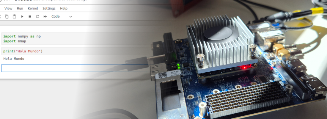
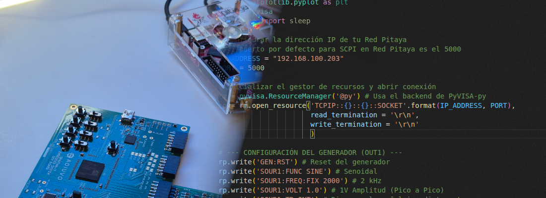
A few weeks ago we talked here about the Red Pitaya STEMlab board. We saw how we can use its web-based environment to deploy different APPS and also how using Python we could read and write analog and digital data to a credit card size board. As I mentioned in that post, the STEMlab is not just a web-based oscilloscope, it is a Zynq development board with a high-speed ADC, a high-speed DAC, and a bunch of GPIO accessible via two 2x10 connectors. In this post, we are going to use the STEMlab not from Python or its web environment, but using the board as a Zynq development board.
First of all, we open the GitHub page from Read Pitaya where we can find all the files needed to play with the FPGA of the board. On that repository, we can find the board file, and several example projects. To regenerate those projects, we need to follow this guide since it is all automatized which is good. In the example projects we can find different projects from a simple LED blinking to a pong game, but in this post, we are not going to use one of those projects but we are going to generate a new project using Vivado 2023.1. The idea of this project is to be able to generate a new HW base design for the board to be used for data processing, programming an oscilloscope, or a signal generator. The diagram of the project will be the next.

Since it is a base project, for the moment I will not add a HW trigger. Later I will explain how we can add it to this design.
First of all, we need to download the board file, and add it to Vivado’s board repository. In my case, I have created a new repository where I added the Red Pitaya files.

Once the board is added, we can create a new project.

The Red Pitaya STEMlab board will appear in the board selection menu, so we can select it for the project.

Once the project is created, since it is a Zynq-based project, we are going to use the block design to implement our design. In the block design, the first block we are going to add is the Zynq PS.

Now, when the board preset is applied, we are going to make some changes in the Zynq PS configuration. First of all, we need to add an AXI HP Slave port. This port later will be connected to the DMA. Also, the width of the port has to be changed to 32 bits.

In the board configuration, the PS is configured to generate a 50 MHz for the PL. For this project, we are going to increase that frequency to 100 MHz.
When the PS is configured, we can add the block AXI Direct Memory Access to the block design. We will keep the configuration of the DMA very simple, so we are going to disable the Scatter Gather Engine, but we do need to keep the read and write channels. The read channel will be used to read data from the ADC, and the write channel will be used to write data into the DAC. Then, let Vivado connect the DMA and some blocks will be added to the block design. The result will be similar to the following.

Now it’s time to add the FIFO memories. We will need two FIFO, one for the ADC and another one for the DAC, but the configuration of both will be the same. We will configure a fixed depth of 16k samples. Also since the ADC works at 125 MHz, and our system works at 100 MHz, we will need to configure different clocks for both channels of the memory.

Although part of our design will work at 125 Mhz, we don’t need to generate this clock because the STEMlab has a clock connected to the ADC. This clock is sent to the Zynq so we can use this input clock.

Now, when the FIFO memories are connected to the DMA, the last step will be to add the ADC and DAC drivers. The converters used in the board are very similar to the ones used in the ZMOD ADC and ZMOD DAC, however, they are not exactly the same pieces, and also, the configuration of the ADC is quite different since it does not work in DDR mode, but it uses two different parallel ports to read the data.
I have designed the drivers following the examples provided by Red Pitaya, but you can use their drivers without any problem. Adding the drivers to the design, the complete block design is the next. Notice that both ADC and DAC use the clock provided by the ADC, so the sampling frequency is fixed at 125 MHz.

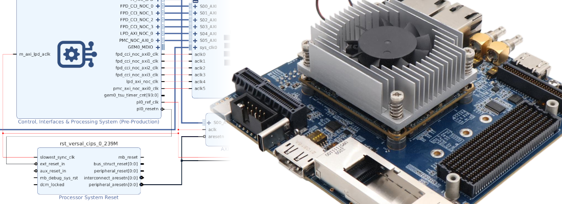
If we need to add a HW trigger, the design will change a bit. First, we need to add a STEMlab trigger module configured over AXi to let the user change the trigger level. Also, we can develop our own FIFO memory where the data depth will be configurable. In addition, since we have more modules to configure over AXI4 Lite, an AXI Interconnect has to be added. The diagram could be the following.

We can say that boards like the Red Pitaya STEMlab are boards for everybody. If you just want an oscilloscope or a signal generator, you can use this board. If you are a validation engineer who needs to generate and read different analog or digital patterns from your Python script, this board will be also useful for you, finally, if you are an FPGA designer and need a board with a high-speed ADC and DAC, it is also your board, but in this case, you will need to solder the JTAG interface pins since it has not an integrated USB-JTAG.