Creating an AXI Stream IP for an acquisition system.
 Eclypse Z7
On the last post, we talk about the using of DMA to send data between PL and PS on SOC or MPSOC devices. The example that I proposed, was a kind of FFT compute accelerator, where a signal stored on the DDR was sent to the PL, and here, an FFT was computed, then, the result of the FFT was sent again to the DDR to make data accesible from the PS.
Even that is a good example of acceleration, if we talk about signal processing, a complete signal processing system also includes the acquisition. This time I will show you how to develop the entire acquisition system, including acquisition, processing and storage.

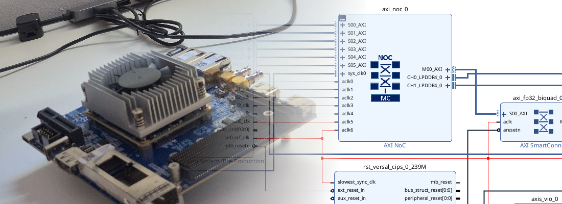
The diagram of this system is a bit more complex than the diagram described on the last post. This time I have included an AXI Stream IP to manage the Digilent’s ZMOD ADC data, 2 FIFO memories to hold data, and a third DMA channel to send data directly from ZMOD to DDR. Also 2 AXI Lite interfaces are added to configure the new DMA, and the ZMOD ADC IP. The goal of this system is to acquire 2 signals with ZMOD ADC, one of them will be sent to an FFT IP for compute the DFT of the signal and sent the result to the DDR. The other acquired signal will be sent directly to be processed by the PS.
For this project I have used the Eclypse Z7 board, that is based on Zynq 7000, instead of TE0802 that is based on Zynq US+. Zynq 7000 devices have differences in terms of interfaces between PL and PS, but they still have the High Performance interfaces with direct access to DDR, and General Purpose interfaces with their own addresses to configuration.
Let’s start with the acquisition system. To create the AXI Stream IP for ZMOD ADC manage, I have create a new AXI4 IP, and when we are on Add peripherals window, we have to add 2 more interfaces. At the end, the new IP will have one AXI4 Lite interface for configuration, with 4 registers in my case, and 2 AXI4 Stream interfaces to send signals data.

Once we have the AXI IP created, we need to add our own code to the IP. In general, when I create an AXI4 Lite IP, I use the code generated by Vivado to manage the communications, in this case, on AXI4 Lite communication, I will use the code generated by Vivado, but I am going to delete the code generated by Vivado to manage the 2 AXI4 Stream communications, because this interfaces will be managed by my own code. The reason to do that is essentially that, AXI Stream interface is very easy to implement, and this give us more freedom to implement modifications. On AXI4 Stream interface there are only 4 signals to manage, tvalid, to indicate the slave that there are a new data available on the bus, tready, to indicate the master that slave is ready to accept data, tlast, to indicate to slave that the data frame is finished (this is optional and we only will use it to the xFFT IP), and tdata, with data itself.
Data from the ZMOD is not directly driven to the xFFT and the DMA, but is sent to FIFO memories. I should include these FIFO memories because sometimes, on the frame sent from ZMOD AXI IP to the DMA, DMA clears the tready signal at the middle of the frame. This is not a problem if we have the signal stored, but in this acquisition system, this event makes the signal non continuous, so data is not valid to apply a processing algorithm. Also, I had to change the acquisition logic. In general, when the master sets the trigger on, samples are acquired. On this system, samples are sent to the FIFO always, and when master sets the trigger on, samples stop to be stored, and data on FIFO remains stable during the reading process. Once the entire FIFO is read, data is updated again.
This method could be valid or not according to the goal of the system, but in general, when we want to compute the FFT, we assume that it is not a real time processing, because FFT is computed for an amount of data, not only for the last ones. In case that we need a real time FFT compute, the schema created on this post will change.
The system with ZMOD ADC, FIFOs, xFFT and DMA is shown in the next figure.

And the complete block design will be shown on the next image.

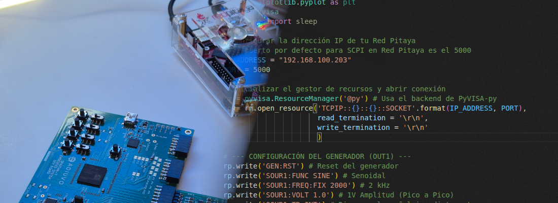
Regarding the SDK project, there are no differences between this projects and the last, since the DMA configuration is the same.
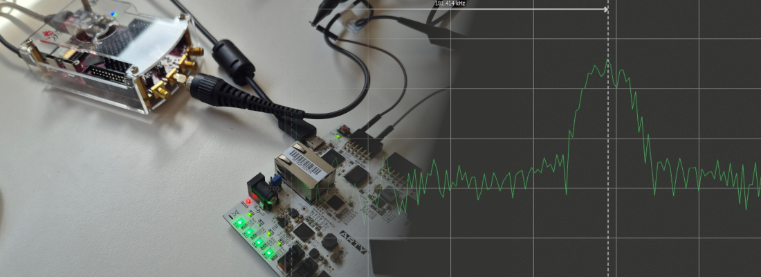
With this project we will have an entire acquisition system based on AXI Stream interface. Using this standard, we can develop filters or detectors and integrate it in our design easily. Vivado offers us a FIR filter based on AXI Stream, the [FIR compiler IP[/2020/11/09/using-xilinxs-fir-compiler/], that is very interesting because it made really easy to implement a FIR filter, and add it to our design. As a test, you can add it on the path between AXI ZMOD ADC and the xFFT to clean the spectrum.