Discovering Gowin FPGA.
A few weeks ago Dialog Semiconductor announced a new series of FPGAs named ForgeFPGA. The highlight of these new devices are not high processing power, the highest speed or the big they are, the main highlights of these devices are Low-Power and Low-Cost. This kind of announcement shows us the way of the new FPGAs. The main point is that there is a place for small FPGAs with low consumption and also very affordable prices (<10$). In this area, we can find some devices from the main FPGA manufacturers, but also some other manufacturers that are specialized in this market, like Dialog and Gowin. In this post, I will use an FPGA from Gowin, the Littlebee GW1NSR, and I will analyze from my point of view its DSP capabilities.
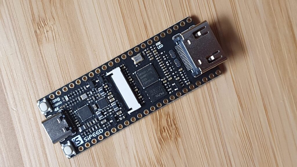
The board I have acquired is the Sipeed Tang Nano 4K. This board is based on the SiP GW1NSR-4C device, which has inside 4k logic blocks and an Arm Cortex M3 processor. This board has access to almost all the pins of the FPGA, that are not a lot since the FPGA is packaged in a QFN48. In addition to the pin headers, the board has an HDMI connector and a MIPI camera socket.
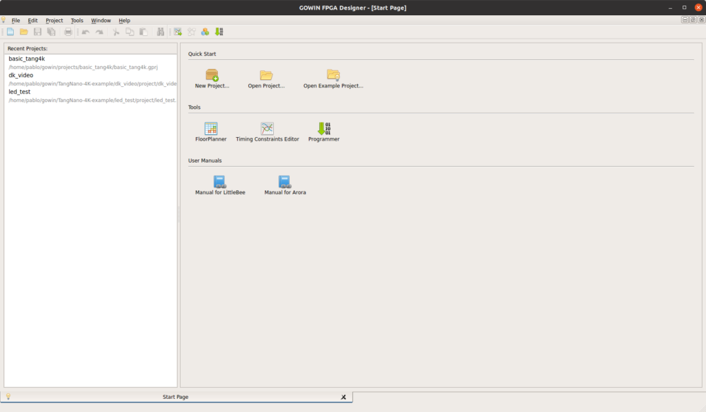
To develop for this board, Gowin has its IDE that is free, but you must request a license from their webpage. In Linux, the entire IDE is portable and has a size of 1.1GB, which is very small compared with other FPGA IDEs.
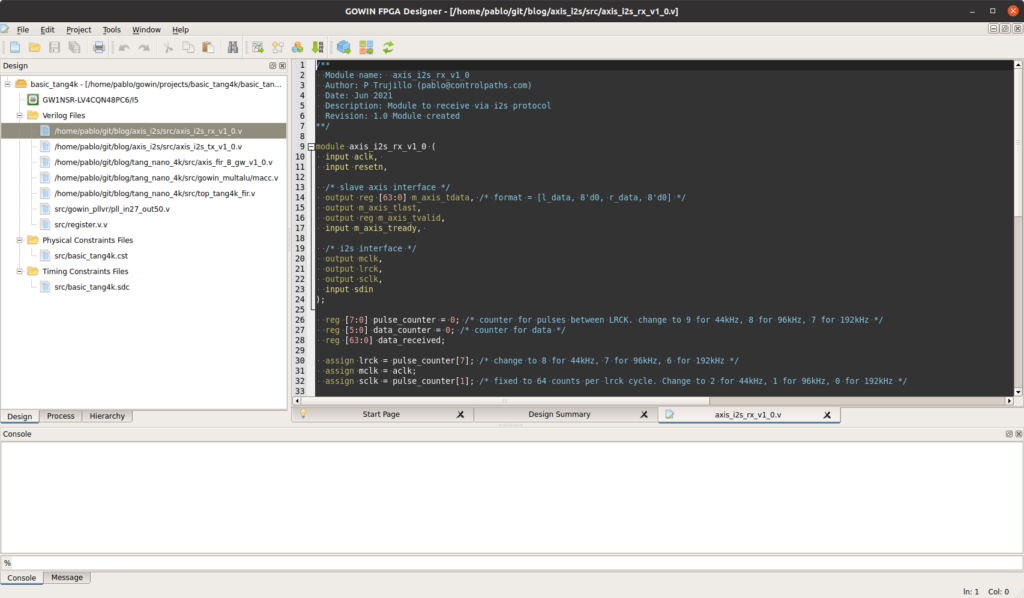
The IDE has all that you could expect from an IDE, no more and no less, including a set of IP Cores that offers at no cost IP for MIPI CSI, RGB to HDMI, PCI target or even USB 2.0 Device Controller. For some reason, for the GW1NSR device, the FIR and the IIR filters are not available(?).
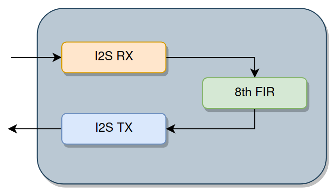
To test the device in my favorite field, the DSP, I have designed a simple audio processing system, where a signal is acquired through an I2S interface (this interface is neither included in the IDE), then this signal is filtered with an 8th order FIR filter, and then is getting out again through a TX I2S interface.
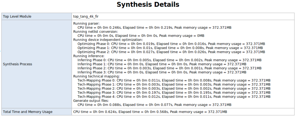
I know that is a very simple design but I expect the synthesis process to take at least 10 to 20 seconds, but the process only takes 0,624 seconds… That’s less than the time it takes my colleagues who program the Arm to compile a Hello World!
The next in the FPGA development flow is the Place and Route process. This time the time taken by the IDE is 5 seconds.
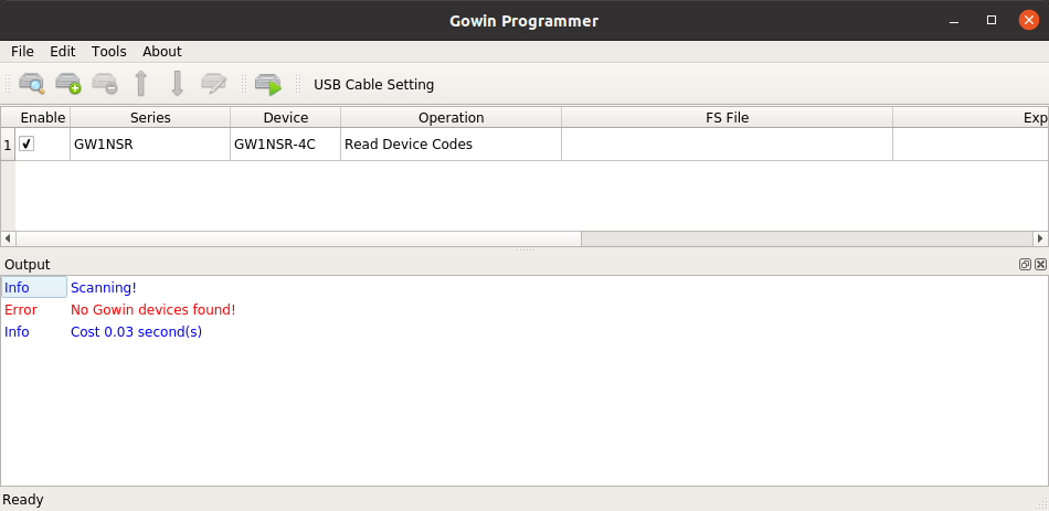
Once the design is synthesized, the next is to program the device. At this point I found some issues with the board detection from the Programmer application from Gowin, even executing it as a root user.
Fortunately, I found an open source project to program the FPGA, OpenFPGALoader, and is available for Windows and Linux. When the application is installed, executing it with the argument –detect the tang nano 4k is detected correctly.
~/gowin$ openFPGALoader --detect
write to ram
Jtag frequency : requested 6.00MHz   -> real 6.00MHz
index 0:
	idcode 0x100981b
	manufacturer Gowin
	family GW1NSR
	model  GW1NSR-4C
	irlength 8
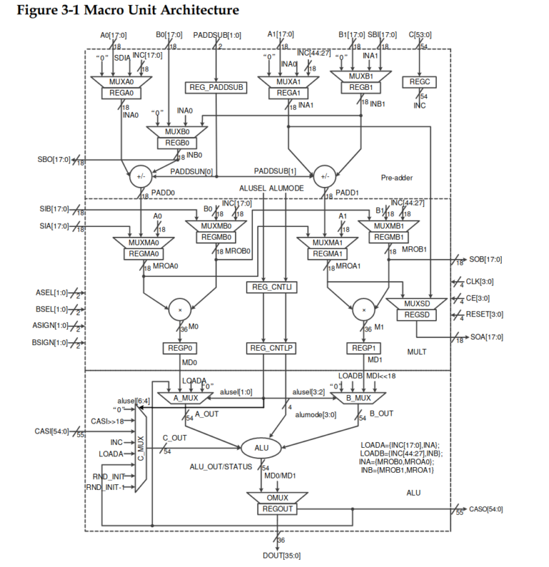
Great, at this point, we already can develop and program the Tang Nano 4K, now, what about their DSP capabilities? If we check the documentation of the GW1NSR devices, we can see that for the 4C variant, the number of available 18×18 multipliers is 16. This amount of multipliers is built in DSP blocks of 2 18×18 multipliers together, with 2 pre-adders, and one ALU at the output of the multipliers. Each of these blocks can be configured only to multiply signals of 9×9, 18×18, 18×36 and 36×36 (at least in my configuration I could not perform a multiplication out of this bounds).
And this is related to the next. In the Verilog code of my FIR filter, the multiplication blocks are inferred, there is not an instantiation of the MACC os DSP block, simply I use the symbol ‘*’ to tell the synthesizer that there it has to infer a MULT block. In this case, all the signals have a width of 16 bits.
/* MACC structure */
assign input_b0 = input_pipe0 * b0_int;
assign input_b1 = (input_pipe1 * b1_int) + input_b0;
assign input_b2 = (input_pipe2 * b2_int) + input_b1;
assign input_b3 = (input_pipe3 * b3_int) + input_b2;
assign input_b4 = (input_pipe4 * b4_int) + input_b3;
assign input_b5 = (input_pipe5 * b5_int) + input_b4;
assign input_b6 = (input_pipe6 * b6_int) + input_b5;
assign input_b7 = (input_pipe7 * b7_int) + input_b6;
assign input_b8 = (input_pipe8 * b8_int) + input_b7;
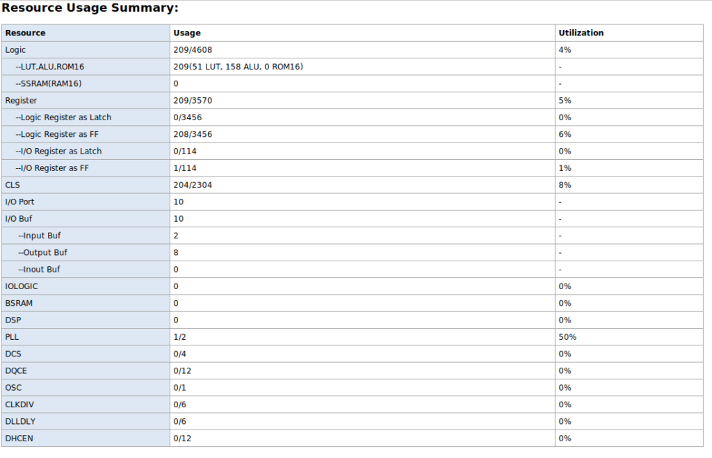
When we implement that, the result is shown below.
We can see that the DSP blocks used are 0, on the other hand, there are 158 logic blocks configured as ALU. These Configurable Logic Units (CLU) can perform multiplications, as you can see in the datasheet of the device, on page 15(89), where the configurations of the CLU are explained. I tried also to change the structure of this block, in order to force the use of DSP blocks, by changing the polarity of the reset and adding a clock enable signal to the multiplication with the same result.
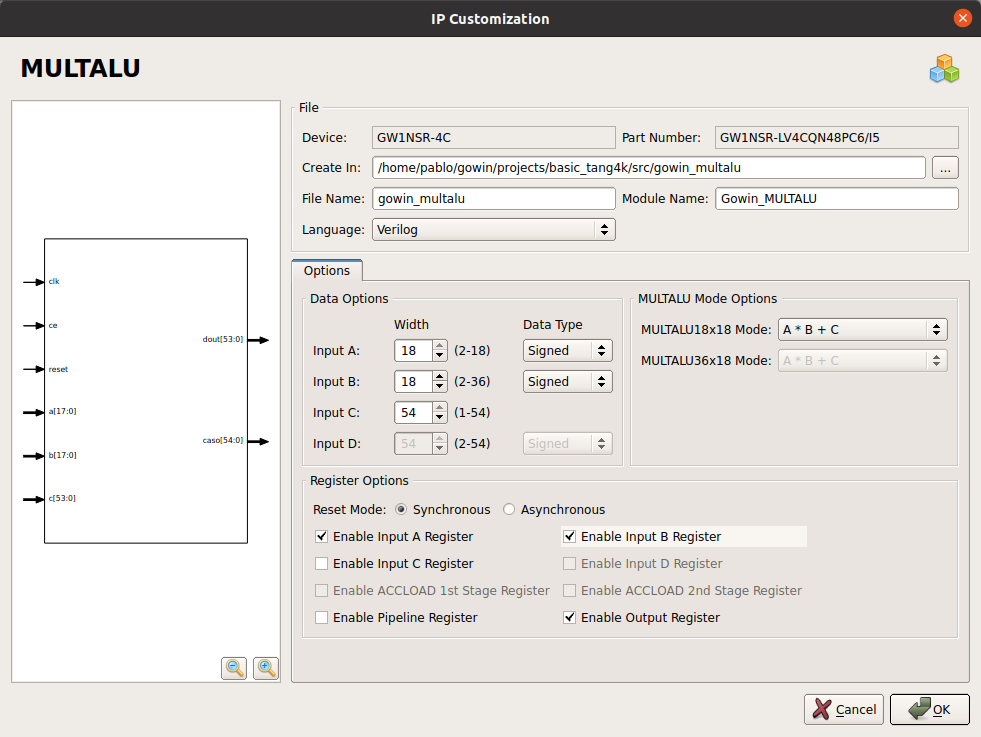
To make the IDE use the available DSP blocks, we have to include in the design the corresponding IP with the operation that we want to perform. To use the DSP blocks to implement the FIR filter, we have to configure the block to perform a multiplication followed by an adder. This operation can be performed by the IP MULTALU.
In the configuration, we select the width of the inputs, and the configurator will select the appropriate configuration for the DSP block. If the widths of the inputs are less than 18, only one multiplicator will be used, and the IP used will be MULTALU18x18. If one of the inputs exceeds the width of the IP, the configurator will change to the IP MULTALU36x18, and both multiplicators of the DSP block will be used.
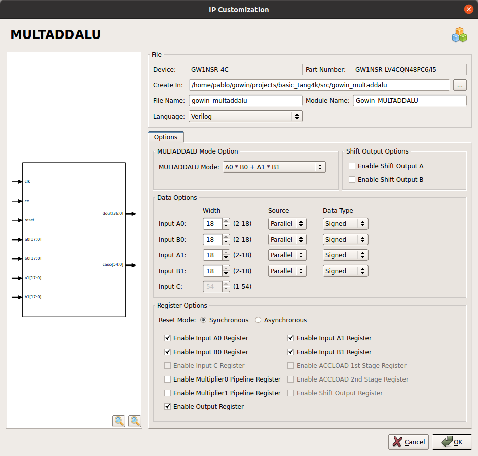
In the case that only one multiplier was used, the other one cannot be accessible if we use this IP, in other words, we are misusing the device. To force the use of both multiplicators, the IP we have to use is MULTADDALU.
In this case, 2 multiplications are performed, but the width of each one can not exceed 18 bits. Then, the result of both multiplications can be added or subtracted.
To implement the 8th-order FIR filter, we have to develop the Verilog module considering the limitation in the width of each IP. For internal widths of 18 bits or less, we can use the 4xMULTADDALU, and the outputs have to be added using logic. In the case of symmetric coefficients, we can use only 2. On the other hand, if the internal width of the module is greater than 18 bits, the structure of the FIR filter changes completely, since a different IP has to be used. In case of a width greater than 36 bits, the FPGA will use the logic to implement the operations, which is less optimized.
At this point, I can ask you, Will you use this FPGA for digital signal processing? For me, the answer is clear, absolutely yes! Even this model with only 8 DSP blocks (16 multipliers), can be an excellent partner to perform filtering (we can use folding, or an FFT, always knowing its limitations. I see this FPGA as a couple of a processor, running high-speed signal processing and communicating with the processor via SPI.
As we always say in the blog, this kind of FPGA is one more tool we have to use in our developments, and it is up to us to use them in the right development.


