Using PCIe in Xilinx 7 Series.
When we look into communicating an FPGA with a computer, the first interface that we can find is UART, but this interface has several limitations in terms of speed. In order to transfer a high amount of data between the CPU and an FPGA, we will need to use some more sophisticated interfaces like PCI Express (PCIe). Graphics cards and ethernet cards are both examples of peripherals that use this interface to interchange data with the CPU through PCIe. This interface uses one or more differential lines, each one called lane (x1, x4, x8 and x16), to transfer data at speeds up to 252 Giga Transactions per Second in the case of using the fourth generation of the interface and 16 lanes. PCIe has become a very common interface for high-end FPGA, but it can be found also in mid-range FPGA like Zynq. According to the FPGA we are going to use, the number of lanes and the speed will change. In this post we are going to use the Picozed 7015 board with the FMC Carrier board v2 that includes a PCIe gen2 x1 connector, that can achieve speeds up to 3.25 Gbps according to their speed grade.
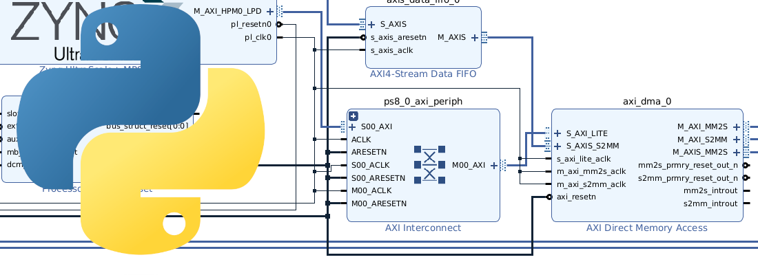
In order to implement high-speed interfaces, FPGA has dedicated hardware. In the case of Xilinx FPGA, we can find in some parts different types of Multi-Gigabit Transceivers (MGT), each one with differences in speed or capabilities. For Zynq 7015 we have 4 GTP transceivers. Besides the use of dedicated hardware, in order to use these interfaces we usually will use specific IP cores. In the case of the PCIe interface Xilinx allows to use it free of charge of different IPs. For this post, I used the DMA/Bridge Subsystem for PCI Express. This IP can act as an AXI4 Lite master, allowing the fabric can be accessed by the CPU host. MGT also includes the needed hardware to manage high-speed clocks (Reference clocks). As the clocks are part of dedicated hardware, when we connect the clock inputs in the block design, we have to do it through a IBUFDS_GTE2 primitive, and leave unconnected the output IBUF_DS_ODIV2 for this board. To instantiate this primitive in block design, we have to add a Utility buffer, and then select the corresponding buffer type. The entire block diagram is shown in the next figure. We can see the input reference clock, the DMA/Bridge IP, and then an AXI Interconnect that connects the M_AXI_LITE port of the DMA Bridge, to an AXI GPIO connected to the 4 LEDs of the board, and also to an AXI BRAM controller.

Regarding the configuration of the DMA Bridge, as the board only has connected to the PCI port 1 lane, we have to select a Lane Width of X1, and the reference clock frequency as the standard clock speed for PCI, which is 100MHz. Regarding the Maximum Link Speed, this part only can be selectable at 2.5 GT/s.

For the rest of the tabs, we can take a look to the PCIe ID tab, where we can find the IDs of the device that later we will find from the OS. Also, in BARs tab, we can enable the AXI Lite Master Interface, and apply a translation between PCIe addresses and AXI addresses. To configure this value, we will notice that the address we will see from de Operating system is different than the addresses of the AXI bus. When we set the “pointer” to the address of the OS, then this address starts at 0, so the AXI address corresponding will be 0.

Checking the Address Editor we can see that the addresses starts at 0x8000_0000, so we will configure this value as PCIe to AXI Translation.

When the design is synthesized, we can assign the IOs. For the PCIe, the corresponding pins can be found in the hardware user guide of the FMC Carrier v2.

set_property PACKAGE_PIN U9 [get_ports pcie_refclk_p]
set_property LOC GTPE2_CHANNEL_X0Y0 [get_cells {picozed_pcie_bd_i/xdma_0/inst/picozed_pcie_bd_xdma_0_0_pcie2_to_pcie3_wrapper_i/pcie2_ip_i/inst/inst/gt_top_i/pipe_wrapper_i/pipe_lane[0].gt_wrapper_i/gtp_channel.gtpe2_channel_i}]
set_property PACKAGE_PIN AB7 [get_ports {pcie_7x_mgt_rtl_rxn[0]}]
set_property PACKAGE_PIN V13 [get_ports pcie_rstn]
set_property IOSTANDARD LVCMOS33 [get_ports pcie_rstn]
Once the design is implemented, we can connect the board to a PCIe socket, and, before turning on the PC, we must configure the FPGA. This is because the enumeration of the PCIe peripherals is made by the BIOS in the power-up of the PC. I have used a Linux distribution because is simplest than using Windows, but the result must be the same.
First, we will execute the command lspci with verbose option in order to obtain the maximum information of the PCI peripherals connected.
~$ lspci -vvv
The output of this command will show all the PCIe peripherals, and one of them will be a Xilinx device. We can see that device 7011 is the same id configured in the DMA Bridge IP. Regarding the memory allocation, we can see 2 addresses range. The address range that is corresponding to the AXI Master interface is the one that has a size of 1M, that is corresponding with the size configured in the BARs tab of AXI Bridge IP.
02:00.0 Serial controller: Xilinx Corporation Device 7011 (prog-if 01 [16450])
	Subsystem: Xilinx Corporation Device 0007
	Control: I/O- Mem+ BusMaster- SpecCycle- MemWINV- VGASnoop- ParErr- Stepping- SERR- FastB2B- DisINTx-
	Status: Cap+ 66MHz- UDF- FastB2B- ParErr- DEVSEL=fast >TAbort- <TAbort- <MAbort- >SERR- <PERR- INTx-
	Interrupt: pin A routed to IRQ 19
	Region 0: Memory at b1000000 (32-bit, non-prefetchable) [size=1M]
	Region 1: Memory at b1100000 (32-bit, non-prefetchable) [size=64K]
	Capabilities: <access denied>
To manage the PCI interface, I have developed a very simple driver in Python that uses the libraries mmap and os.
import mmap
import os

# open entire host memory
f = os.open('/dev/mem', os.O_RDWR)

# map memory section according pci assignment. 0x17fff is corresponding with AXI GPIO + BRAM address.
m = mmap.mmap(f,0x17FFF, flags=mmap.MAP_SHARED, prot=(mmap.PROT_READ|mmap.PROT_WRITE), offset=0xb1000000)

# Point to first address of the region
m.seek(0)

# write first address of the region. AXI GPIO
m.write(b'\x05')

# Pointer has been increased. Return the the first address.
m.seek(0)

# blink leds
m.write(b'\x0a')
That PCIe is one of the most powerful interfaces in a PC is obvious, but this interface is also very scalable since we can use it from 1 lane to 16. For this example that I have developed for this post, we only have communication with the board, so 1 lane is more than we need, but in some cases where we need to write or read a large quantity of data, like graphics cards, even 16 lanes can be a bottleneck with the new processors and the new high-end FPGAs. With this post, I hope to open a new series of posts using this interface and try to extract some of the potential of this interface with the Picozed board and some new boards.