Streaming data to DDR memory from PL on Arty board.

 Arty A7
In the last article, we talked about using the AXI Datamover IP, which allows us to perform DDR memory transactions in a way very similar to how we would with an SoC and AXI DMA. The article used the YPCB-00388-1P1 board to transfer data from PCIe to DDR memory.
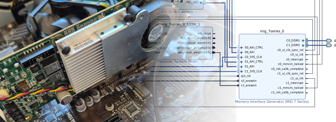
This setup introduces two different clock domains in the design, which makes the use of Clock Domain Crossing (CDC) techniques necessary. To simplify the design and reduce the number of clock domains to just one, I created a project targeting the Arty board. However, it can be used with any 7-series board that has DDR memory attached.
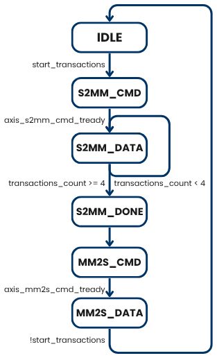
To manage the AXI Datamover IP, I used the following finite state machine (FSM).
First we need to write on the S2MM command interface in order to transfer data from the AXI4 Stream interface to the DDR3 memory. According the AXI Data Mover User Guide, the structure of this command is the one we can see in the next figure.
The width of the command data interface depends on the width of the address, as specified in the AXI Datamover User Guide (Section 3.2). For a 32-bit address, the command width is calculated as 72 bits, which includes fields for the tag (4 bits), address (32 bits), DDR (1 bit), EOF (1 bit), DSA (6 bits), type (1 bit), and BTT (23 bits).
/* cmd structure:
| Field   | Bits | Description          |
|---------|------|----------------------|
| 4'd0    | 4    | Reserved             |
| tag     | 4    | Command TAG          |
| sddr    | 32   | Start Address              |
| ddr     | 1    | DRE ReAlignment Request      |
| eof     | 1    | End of frame flag    |
| dsa     | 6    | DRE Stream Alignment |
| type    | 1    | Transfer type        |
| btt     | 23   | Bytes to transfer    |
*/
assign axis_s2mm_cmd_tdata = {4'd0, s2mm_cmd_tag, s2mm_cmd_saddr, s2mm_cmd_ddr, s2mm_cmd_eof, s2mm_cmd_dsa, s2mm_cmd_type, s2mm_cmd_btt};
The structure is the same for both S2MM and MM2S channels.
In the next lines, you will find the Verilog code implementing the FSM states.
case (fsm_state)
  3'b000: begin // idle state
    axis_s2mm_cmd_tvalid <= 1'b0;
    axis_s2mm_tvalid <= 1'b0;
    transaction_count <= 4'd0; // reset transaction count
    if (start_transactions) begin
      fsm_state <= 3'b001; // move to command state
    end
  end

  3'b001: begin // command sending state
    axis_s2mm_cmd_tvalid <= 1'b1;
    if (axis_s2mm_cmd_tready) begin
      fsm_state <= 3'b010; // move to data state
    end
  end

  3'b010: begin // data sending state
    axis_s2mm_cmd_tvalid <= 1'b0; // stop sending command
    if (transaction_count < 4'd4) begin // 4 transactions
      if (axis_s2mm_tready) begin
        axis_s2mm_tdata <= axis_s2mm_tdata + 1; // increment data for each transaction
        transaction_count <= transaction_count + 1;
        axis_s2mm_tvalid <= 1'b1; // send data
      end
    end else begin
      axis_s2mm_tvalid <= 1'b0; // stop sending data after 4 transactions
      fsm_state <= 3'b011; // move to completion state
    end

  end
  3'b011: begin // completion state
    axis_s2mm_tvalid <= 1'b0; // stop sending data
    axis_s2mm_cmd_tvalid <= 1'b0; // stop sending command
    fsm_state <= 3'b100; // move to mm2s command state
  end

  3'b100: begin // command sending state
    axis_mm2s_cmd_tvalid <= 1'b1;
    if (axis_mm2s_cmd_tready) begin
      fsm_state <= 3'b101; // move to data state
    end
  end

  3'b101: begin
    axis_mm2s_cmd_tvalid <= 1'b0; // stop sending command
    if (!start_transactions)
      fsm_state <= 3'b000; // go back to idle state if no transactions are requested
  end

  default: begin
    fsm_state <= 3'b000; // reset to idle state on unexpected state
  end

endcase
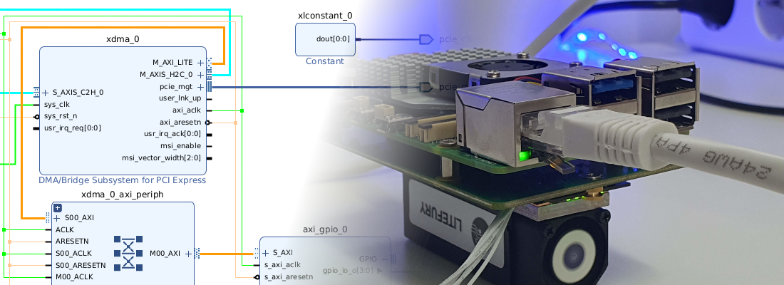
The block design in this case is simpler than the one we saw in the last article. Here we only have one clock domain, provided by the clock generated by the Memory Interface Generator (MIG7). The blocks used are the MIG7 to manage the Memory interface, the AXI Datamover and the custom module axi_config_datamover to manage and generate the transaction for the AXI datamover. Also you can find a reset generator, and Integrated Logic Analyzer (ILA) for debugging, and finally an Virtual-input-output (VIO) to start the transactions through the JTAG.
Regarding the configuration of the AXI datamover IP, we have two differet tabs. In the first tab we need to check that the Enable xCACHE xUSER checkbox is disables. This configuration extends the command interface with these two fields.
In the second tab, we are going to activate the checkbox Enable Single AXI4 Data Interface. This is optional, but it simplifies the blockdesign by using just one AXI4 Master interface.
Now, we need to use Vivado to generate the wrapper and bitstream. First, open the Vivado project, navigate to the “Flow Navigator” pane, and click on “Generate Bitstream” under the “Program and Debug” section. Once the bitstream is generated, connect the Arty board to your computer via JTAG, and use the “Program Device” option in Vivado to load the design onto the board.
In the ILA, we can configure the tvalid signal of the S2MM AXI-Stream interface as a trigger. To do this, open the ILA configuration in Vivado, select the tvalid signal from the list of monitored signals, and set it as the trigger condition. You can specify whether the trigger should activate on a rising edge, falling edge, or a specific value of the signal. Once configured, when the signal start_transactions is set, the ILA will capture and display all the transactions.
First, we can see the S2MM Command transaction, where the axi_config_datamover configures the S2MM channel, and just after this transaction the AXI-Stream sending data to the AXI4 Datamover. Once the S2MM transactions finishes, we can see the MM2S command transaction, however the AXI4 Master interface remains in idle state. Some clock cycles after the MM2S command has been sent, the AXI4 master execute the Write transaction in the DDR. Then, the MM2S transaction is executed in the AXI4 Master interfacre, and finally data is sent over the AXI Stream interface.
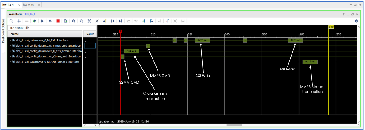
The AXI Datamover uses an internal FIFO memory to temporarily store data before sending it to DDR memory. This behavior can cause the commands to appear out of order. From the point of view of the AXI4 Stream interface, we will not notice this.
Using the AXI4 Datamover on the Arty A7 platform shows how high-performance memory transfers can be achieved without relying on a processor. By leveraging the flexibility of the FPGA, we built an efficient architecture to move data between peripherals like PCIe and DDR memory, while simplifying the design and avoiding clock domain issues by using a single clock source.