Connecting an FPGA accelerator to the Raspberry Pi 5
 Litefury
Since the first version of Raspberry Pi was released in 2012, four more versions of this Single Board Computer (SBC) were released. The fourth version came with a new feature that increased the power of that SBC. That version was the first with PCIe interface (just the CM4 version), although we had to wait for the fifth version, the Raspberry Pi 5, to have that feature on the regular board. Having a PCIe interface accessible to the processor means a lot of things. First, we can use NVME hard drives as a primary storage unit, also the (limited) use of an external graphics card is now possible. Notice that I used the word limited. The reason is that the PCIe interface available in the Raspberry Pi 5 has just one lane, and can achieve up to 8 GT/s, so we have available a PCIe gen3 x1. Is this slow? Not at all, we can use this interface for many different things, and, being this one a blog about FPGA, that is exactly what we will use.
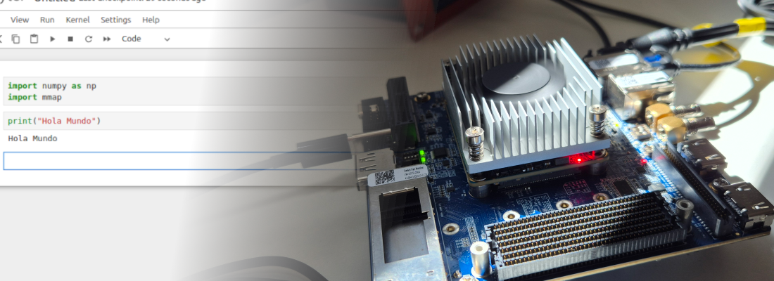
For this article, I am going to use the Litefury board. This board features an Artix XC7A100T with an M.2 format. To connect the board to the Raspberry Pi I will use the Pineberry HAT Drive Bottom. This hat uses the PCIe x1 connector of the Raspberry PI 5 (RP5) and is connected to an M.2 socket. It is intended for SSD but it works well with the Litefury. When I started this article, I was concerned about the power consumption of the Litefury, but I was able to use the bard without any external supply. As an operating system for the Raspberry Pi, I used the Raspberry Pi OS server edition.

When we power on the RP5 for the first time, we need to modify the config.txt file to enable the PCIe interface. This file is located at /boot/firmware/config.txt. To enable the PCIe we need to add the next line.
# Enable the PCIe external connector.
dtparam=pciex1
This configuration enables the PCIe interface but with a limited speed of 5 GT/s (gen2), but by adding another instruction we can increase the speed to 8 GT/s (gen3). For this project this is not useful because the Artix7 used in the Litefury can only be configured for gen2, so this will be enough.
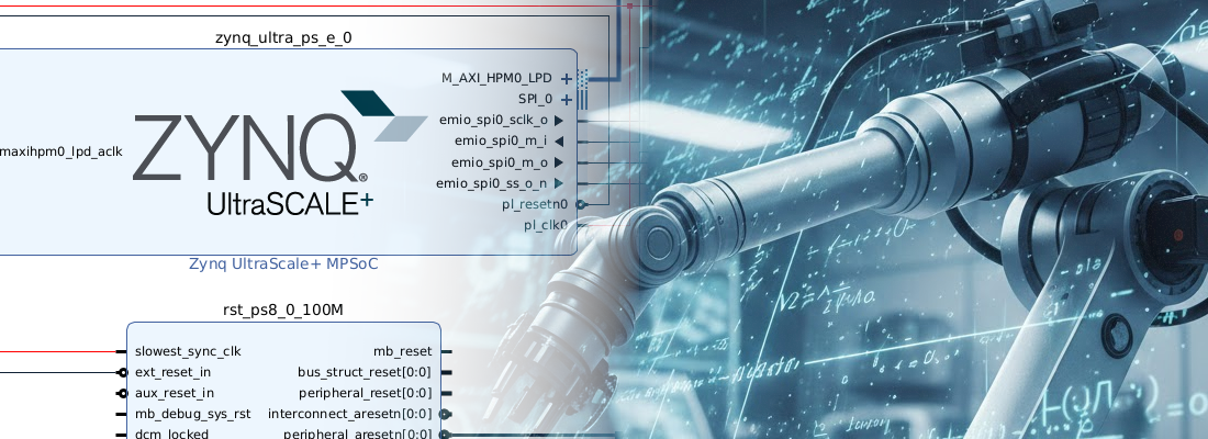
Once the RP5 is configured, is time to create the FPGA design. When the project for the XC7A100t-2LFGG484 part is created, and a new block design is added to the project, we need to add the DMA/Bridge Subsystem for PCI Express IP.

When this IP is added to the block design, we can configure it through a wizard. The configuration is the one you can see in the next figure. We are going to use just one lane of the PCIe, 5 GT/s and the DMA interface will be set to AXI Stream, with just one channel for read and write.

When the basic configuration is done, a BUffer for the PCIe clock will be added automatically. Now, that the basic configuration of the IP is finished, we can go into the configuration of the IP, and change other parameters, like the PCI Class Code, which will be set to 120000. The rest of the configuration can be the default one.

Now it is time to add some other IP to the design. The project will be very simple. We are going to use the AXI Stream interface to read and write an AXI4-Stream Data FIFO. Then, the AXI4 LITE Master interface will be connected to an AXI GPIO IP that controls the four LEDs of the board. Also, we need to add the port pcie_clkreq_l, and assign it a value of ‘0’. The entire block design is shown in the next figure.

Regarding the constraints, we can divide the constraint into two different files, and change the processing order. The reason is that Litefury does not use the default pins for the PCIe lanes, so when the DMA/Bridge Subsystem for PCI Express IP is synthesized, it generates its own constraints which are added to the project. Those constraints are not valid for the Litefury, so we need to change it after Vivado implements the IP. To summarize, we need to be sure that our constraints will be processed after all the predefined constraints. The UG896 says the next: The order in which IP XDC files could be processed is, as follows:
- User XDC set to
EARLY - IP XDC set to
EARLY - User XDC set to
NORMAL(default) - IP XDC set to
LATE - User XDC set to
LATE
So we need to set our constraints to `LATE, so they will be read the last one and will be the ones used in the implementation. We can do this by executing this command:
set_property PROCESSING_ORDER LATE [get_files -all ./raspberrypi_litefury/src/late_litefury.xdc]
The constraints that have to be executed last are the ones with the PCIe lane location.
# Late constraints

# PCIe lane 0
set_property PACKAGE_PIN A10 [get_ports {pcie_mgt_rxn[0]}]
set_property PACKAGE_PIN B10 [get_ports {pcie_mgt_rxp[0]}]
set_property PACKAGE_PIN A6 [get_ports {pcie_mgt_txn[0]}]
set_property PACKAGE_PIN B6 [get_ports {pcie_mgt_txp[0]}]

# PCIe refclock
set_property PACKAGE_PIN F6 [get_ports {pcie_clkin_clk_p[0]}]
set_property PACKAGE_PIN E6 [get_ports {pcie_clkin_clk_n[0]}]

# Other PCIe signals
set_property PACKAGE_PIN G1 [get_ports {pcie_clkreq_l[0]}]
set_property IOSTANDARD LVCMOS33 [get_ports {pcie_clkreq_l[0]}]

set_property PACKAGE_PIN J1 [get_ports pcie_reset]
set_property IOSTANDARD LVCMOS33 [get_ports pcie_reset]
Also, there will be another set of constraints for the LEDs and some instructions to reduce the configuration time.
## Normal constraints

# LEDs

set_property PACKAGE_PIN G3 [get_ports {leds[0]}]
set_property IOSTANDARD LVCMOS33 [get_ports {leds[0]}]
set_property PULLUP true [get_ports {leds[0]}]
set_property DRIVE 8 [get_ports {leds[0]}]

set_property PACKAGE_PIN H3 [get_ports {leds[1]}]
set_property IOSTANDARD LVCMOS33 [get_ports {leds[1]}]
set_property PULLUP true [get_ports {leds[1]}]
set_property DRIVE 8 [get_ports {leds[1]}]

set_property PACKAGE_PIN G4 [get_ports {leds[2]}]
set_property IOSTANDARD LVCMOS33 [get_ports {leds[2]}]
set_property PULLUP true [get_ports {leds[2]}]
set_property DRIVE 8 [get_ports {leds[2]}]

set_property PACKAGE_PIN H4 [get_ports {leds[3]}]
set_property IOSTANDARD LVCMOS33 [get_ports {leds[3]}]
set_property PULLUP true [get_ports {leds[3]}]
set_property DRIVE 8 [get_ports {leds[3]}]

# Input reset is resynchronized within FPGA design as necessary
set_false_path -from [get_ports pci_reset]

# Power down on overtemp
set_property BITSTREAM.CONFIG.OVERTEMPPOWERDOWN ENABLE [current_design]

# High-speed configuration so FPGA is up in time to negotiate with PCIe root complex
set_property BITSTREAM.CONFIG.EXTMASTERCCLK_EN Div-1 [current_design]
set_property BITSTREAM.CONFIG.SPI_BUSWIDTH 4 [current_design]
set_property CONFIG_MODE SPIx4 [current_design]
set_property BITSTREAM.CONFIG.SPI_FALL_EDGE YES [current_design]
set_property BITSTREAM.GENERAL.COMPRESS TRUE [current_design]

set_property CONFIG_VOLTAGE 3.3 [current_design]
set_property CFGBVS VCCO [current_design]
Now, we are ready to generate the bitstream, and the FPGA design is finished.
We can now come back to the RP5. To talk with the Litefury through PCIe we are going to use the dma_ip_drivers from Xilinx. The problem is that these drivers are developed for x86 processors, so ARM processors, like the one in the RP5, are not supported, at least in principle. Fortunately, Laurence Barker discovered what makes them incompatible with ARM processors, and we can find in his Github repository a version of the drivers with some modifications that makes them compatible with ARM processors. The changes are very well documented in the readme file, so what I did was download the original drivers from the Xilinx repository, and apply just the first change. Then I installed the drivers following the Xilinx repository instructions and all went fine.
To test the drivers we can execute the script run_test.sh, but it didn’t work for me, neither on the x86 processor I used here, so I executed directly the test using this command.
pablo@raspberrypi:~ $ ./dma_ip_drivers/XDMA/linux-kernel/tests$ sudo bash ./dma_memory_mapped_test.sh xdma0 1024 1 1 1
The test finished well, so I assume that the drivers are installed correctly and indeed, when I list the devices, all the xdma0 devices are shown.
pablo@raspberrypi:~ $ ls /dev
autofs           gpiochip4     mapper     ram12       stdin   tty25  tty44  tty63      vcsa2        video24          xdma0_events_11
block            gpiomem0      media0     ram13       stdout  tty26  tty45  tty7       vcsa3        video25          xdma0_events_12
btrfs-control    gpiomem1      media1     ram14       tty     tty27  tty46  tty8       vcsa4        video26          xdma0_events_13
bus              gpiomem2      media2     ram15       tty0    tty28  tty47  tty9       vcsa5        video27          xdma0_events_14
cachefiles       gpiomem3      mem        ram2        tty1    tty29  tty48  ttyAMA10   vcsa6        video28          xdma0_events_15
cec0             gpiomem4      mmcblk0    ram3        tty10   tty3   tty49  ttyprintk  vcsu         video29          xdma0_events_2
cec1             hwrng         mmcblk0p1  ram4        tty11   tty30  tty5   uhid       vcsu1        video30          xdma0_events_3
char             initctl       mmcblk0p2  ram5        tty12   tty31  tty50  uinput     vcsu2        video31          xdma0_events_4
console          input         mqueue     ram6        tty13   tty32  tty51  urandom    vcsu3        video32          xdma0_events_5
cpu_dma_latency  kmsg          net        ram7        tty14   tty33  tty52  v4l        vcsu4        video33          xdma0_events_6
cuse             kvm           null       ram8        tty15   tty34  tty53  vc-mem     vcsu5        video34          xdma0_events_7
disk             log           port       ram9        tty16   tty35  tty54  vcio       vcsu6        video35          xdma0_events_8
dma_heap         loop-control  ppp        random      tty17   tty36  tty55  vcs        vga_arbiter  video36          xdma0_events_9
dri              loop0         pps0       rfkill      tty18   tty37  tty56  vcs1       vhci         video37          xdma0_h2c_0
fd               loop1         ptmx       rtc         tty19   tty38  tty57  vcs2       vhost-net    watchdog         xdma0_user
full             loop2         ptp0       rtc0        tty2    tty39  tty58  vcs3       vhost-vsock  watchdog0        xdma0_xvc
fuse             loop3         pts        serial0     tty20   tty4   tty59  vcs4       video19      xdma0_c2h_0      zero
gpiochip0        loop4         ram0       shm         tty21   tty40  tty6   vcs5       video20      xdma0_control
gpiochip1        loop5         ram1       snd         tty22   tty41  tty60  vcs6       video21      xdma0_events_0
gpiochip2        loop6         ram10      spidev10.0  tty23   tty42  tty61  vcsa       video22      xdma0_events_1
gpiochip3        loop7         ram11      stderr      tty24   tty43  tty62  vcsa1      video23      xdma0_events_10
Now, it is time to mix the RP5 and the Litefure and see what happens. When I turned on the system for the first time, I listed the PCI devices and a processing accelerator appeared. At this point, I didn’t load my design into the FPGA, so what we are seeing is the example design that comes in the QSPI memory of the Litefury.
pablo@raspberrypi:~ $ lspci
0000:00:00.0 PCI bridge: Broadcom Inc. and subsidiaries Device 2712 (rev 21)
0000:01:00.0 Processing accelerators: Xilinx Corporation Device 7021
0001:00:00.0 PCI bridge: Broadcom Inc. and subsidiaries Device 2712 (rev 21)
0001:01:00.0 Ethernet controller: Device 1de4:0001
To load my design, I used openFPGALoader installed in the RP5 (load through PCIe for another article), so the Digilent HS3 will be connected to the RP5 and I can manage the load remotely. To install openFPGALoader, we just need to install it from the official repositories.
pablo@raspberrypi:~ $ sudo apt install openFPGALoader
Now, the bitstream was generated in my host computer, so I need to send it to the RP5 using the scp command.
pablo@friday:/litefury_rp5/litefury_rp5.runs/impl_1$ scp ./litefury_rp5_bd_wrapper.bit [email protected]:
[email protected]'s password:
litefury_rp5_bd_wrapper.bit                                                                         100% 1770KB  97.9MB/s   00:00
And finally, I can load the design on the Litefury using the next command.
pablo@raspberrypi:~ $ openFPGALoader -c digilent_hs3 ./litefury_rp5_bd_wrapper.bit
empty
Jtag frequency : requested 6.00MHz   -> real 6.00MHz
Open file DONE
Parse file DONE
load program
Load SRAM: [==================================================] 100.00%
Done
At this point, we have all the needed to send and receive packets through PCIe. I am going to use a Jupyter Notebook to develop the application to manage those transactions. To use a Jupyter notebook in the RP5 from another computer we need to redirect the HTTP port that Jupyter will create. To do this, we need to access the RP5 over SSH and redirect the address localhost:8080 of the remote to port 8080 of the host. The way to do that is the next.
~$ ssh -L 8080:localhost:8080 [email protected]
When the SSH connection is established, we can open the Jupyter notebook in the remote computer as sudo. Also, remember to change the port to the redirected in the host.
~$ sudo jupyter-notebook --no-browser --port=8080 --allow-root
Then, opening the URL localhost:8080 on the host computer, we will see the Jupyter Notebook webpage of the RP5, so all that is executed in this notebook is actually executed in the RP5. (An FPGA engineer needs to know about everything).
Now, the Python application. First of all, some imports. The important ones are the os and the struct. The rest are specific for my application.
import os
import struct
from scipy import signal as sig
import numpy as np
from matplotlib import pyplot as plt
Next, we need to define and open the devices where we are going to write and read. Since I only used one channel in the DMA, we just have the **_0 channels available.
# Open devices for DMA operation
xdma_axis_rd_data = os.open('/dev/xdma0_c2h_0',os.O_RDONLY)
xdma_axis_wr_data = os.open('/dev/xdma0_h2c_0',os.O_WRONLY)
Now, I generated a sine signal with 256 points (the FIFO depth is 512), and using the command os.pwrite I will send the points to the Litefury. There is an extra step that uses the struct.pack command. The width of the DMA channels is 64 bits, so we need to send packets with that width. With the pack command, we are converting the list of 8-bit integers into a 256 byte-like elements array of 64-bit values (‘<256Q’).
# writing a sine signal on DMA channel
nSamples = 256
angle = np.linspace(0,2*np.pi,nSamples, endpoint=False)
sig = np.sin(2*angle)*100
sig_int = sig.astype(int)+100

# Write DMA data channel
data = struct.pack('<256Q', *sig_int)
os.pwrite(xdma_axis_wr_data,data,0)
When this command is executed, it returns us the amount of bytes sent, which is 256x8.
Then, we are going to perform the opposite instruction, we are going to read 256x8 bytes from the read channel. The last zero is the offset.
# Read DMA data channel
data_rd = os.pread(xdma_axis_rd_data,2048,0)
data_unpack = struct.unpack('<256Q',data_rd)
plt.plot(data_unpack)
As we did in the sending, we need to unpack the data to obtain again a list of integers. If all works, we can plot the data sent and the data received and it will be the same.
Also, we enabled an extra AXI4 Master that can be accessed through the device /dev/xdma0_user. The way to proceed is the same, but this time we need to use the offset in the pwrite command to write in a specific AXI4 address. Remember that this interface is connected to an AXI GPIO, so writing the offset 0 we will write the value of the output.
# Open User channel for DMA operation
xdma_user_wr = os.open('/dev/xdma0_user',os.O_WRONLY)

# Write DMA User channel
leds = 10

data = struct.pack('<Q',(15-leds)) # leds status are negated
os.pwrite(xdma_user_wr,data,0)
If you have arrived at this point, you can send bursts of data from the Raspberry Pi 5 to an FPGA, and also read them, which means that you can execute algorithms over data read by the Raspberry PI 5 using hardware ergo, you can do hardware acceleration. The power of Raspberry Pi has been increased over the different versions of the board, but improvements like an accessible PCIe interface are a big step, not to connect a RTX 4090, which is useful just in terms of research, however adding hardware accelerators can be the door to use these SBC as powerful computation devices because, many times, in hardware acceleration, the processor is used just to move data. The question, is this like a Zynq device? has an easy answer, no. On Zynq devices, the FPGA and the processor are very integrated, with many different communication channels, but we have to keep in mind that the cost of this setup is less than 200 euros, including the Litefury. As always, the use of this kind of setup depends of your application.
This project is available on Github