Getting started with a Zynq development board. Base PS Design.
 Pynq Z2
A sales representative has given you a Zynq development board, it has even a heat sink! It seems powerful. When he/she leaves your office you run to your desk to connect your new board to the USB or the AC adapter. The board is alive, some LEDs are blinking, seems that it is sending some text over the UART, and also if you push the push-button the LEDs change the blinking pattern! it is definitely powerful. Time to lunch, you put your new board in a drawer, and… it is your only experience with a Zynq7000 device.
The above text describes me a few years ago when my company bought a Microzed board, and since it is a pity that all those boards are in a drawer, in this article I am showing you how you can create your very first project with a Zynq7000 board, but first, what is a Zynq7000?
Zynq7000 is a family of System-on-chip from AMD (before Xilinx). This device features an FPGA, known as Peripheral Logic (PL), and an ARM Cortex A9, known as Processing System (PS). When I am talking about an ARM Cortex A9, I am saying that you have a complete ARM Cortex A9, with all the peripherals and also all the pins, because yes, in the same chip, we have pins from the PS and pins from the PL.
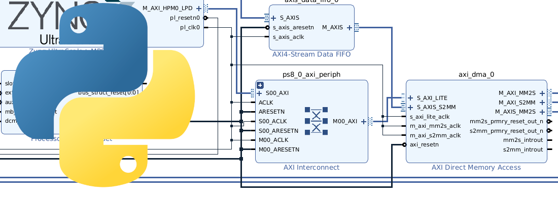
PL and PS can be connected internally over different AXI buses, so we can use the PL to process data and send it to the PS, for example. The possibilities are infinite, but first, we need a starting point. This point will be creating a project that uses the Zynq7000 as an ARM device where we can run a custom C code in the PS. To do this, we are going to use Vivado (to create the hardware project), and then Vitis, to create the software project. The board I am going to use is the Pynq Z2 that features a Zynq 7020 and a bunch of peripherals. I recommend this board because its has all you need from basics projects to more advanced projects, and also its cost, less than 250 Euros.
The steps to start Vivado change according to the operating system you are using. If you are using Windows, you just double-click the Vivado icon on your desktop or look for the Vivado application in the start menu. If you are using Linux, likely you don’t have a shortcut on your desktop, so you have to execute first the script settings64.sh, which is located in the Vivado installation path, and then you just have to type vivado in your terminal.
pablo@miercoles:~$ source /media/pablo/ext_ssd0/xilinx/Vivado/2023.1/settings64.sh
pablo@miercoles:~$ vivado
Now, when Vivado is opened, you will find a window like this regardless you are using Windows or Linux. All the next steps will be the same for Linux and Windows.
In this window, we have several options. The one interesting for us now is Create project.

A new window will be opened, in this window we have to set the name of the project as well as its location. For me, the name of the project will be pynqz2_base.

Now it is time to configure the characteristics of the project. First of all, we need to configure which kind of project we want to create. There are several projects, but in 90% of the cases, we will create an RTL project, which is the standard project where we will add HDL files, we will implement the project, and generate a bitstream. The rest of the projects are used if we have an external tool for synthesis for example. Also, in the RTL project, Vivado asks us whether we want to add source files now, in the project creation workflow, or later, and whether the project is an extensible Vitis platform or not. In this case, we don’t want to specify the source files now, and the project is not an extensible Vitis platform.

Now it’s time to select the hardware we are going to use. In this part, we can specify a part, which is the specific FPGA or Zynq device, or we can select a board. Selecting a board has some advantages like the configuration of the DDR is pre-configured, or some peripherals of the board are also pre-configured so later it will be easy to add them. if we are working with a custom board, usually it won’t be available in the list of boards. These boards are stored in a Git repository, so it is very important to have Git installed in our system to update the catalog.

In this case, we are going to use the Pynq Z2 from TUL Embedded, which is included in the Vivado Boards repository, so we just have to write the name of the board in the search textbox, and then download it. Finally, we have to select the board, and click Next.

Now, the configuration of the project is complete, so the project will be opened, and this will be the window we will see.

To work with a Zynq 7000 device, which has a hardcore that we need to configure, the best is to base the project on a Block Design. In this block design, we will be able to configure the Processing System (PS) using a wizard. Then, if we need to add a custom RTL module, we can add it to the block design and make the corresponding connections. If our project has several RTL modules that are interconnected between them, what I usually do is create a top module in Verilog, and connect all the modules within this top module. Then, the ports of the top module will be the ports available in the block design. In this project we are going to create a project based just in the PS, so we don’t need to add any other module.
To add the processing system to the block design, we can click on the ‘+’ button, and type in the search box Zynq, then a block will appear. Double-clicking in the bloc will add it to the block design.

Here is where we are going to take advantage of using a board that is in the Vivado repository. At the top of the block design will appear a pop-up.

Clicking on Run Block Automation will open a new window.

In this window, we have to check the Apply Board Preset. This option will configure the PS according to the board we are using, from the peripherals available on the board to the configuration of the DDR memory. Now, click on OK, and the icon of our PS in the block design will change to fit the peripherals used. All the peripherals that use pins from the PS will be grouped in the FIXED_IO port, so these peripherals won’t be available in the block design. Also, we can see the port from the DDR, which isn’t available from the PL. In the block design, we will see only the ports that go from the PS to the Peripheral Logic (PL).

To configure the PS, we can double-click over the block and a new window will be opened. In this window, we can see a diagram of the Zynq device with all the peripherals. Those that are enabled will be checked. Also, clicking over one of the peripherals will open the configuration for this peripheral.

The design I want to create in this article is a simple PS project, so we are going to disable all the PS-PL interfaces. To do this we have to open the tab PS-PL Configuration, where we will find all the interfaces between the PL and the PS. This interface uses the AXI standard, and the PL has Master and Slave interfaces. The interface that is enabled by default is a Master General Purpose interface. The configuration for this interface is located on AXI Non-Secure Enablement > GP Master AXI Interface > M AXI GP0 interface. The sentence “AXI Non-Secure Enablement” refers to that the transaction is not part of the ARM’s Trust Zone, so you don’t have to be scared about this, no one hacker will see what you are sending.
OK, since we want to disable all the interfaces, we have to uncheck the interface.

Now, we will see in the block design that the PS block has changed. Now the AXI interface has not shown. The other pins that are shown are the FCLK_CLK0, the FCLK_RESET0_N, and the USBIND_0. The last one is an interface that returns some information about the USB, which is enabled in the ARM so it will appear while the USB is enabled. The other ports can be disabled by disabling the PL clock and the PL reset.

In many of the Zynq boards, there is just one oscillator that is connected to the PS. Then, the clocks for the PL are generated by the PS and connected internally to the PL. In this case, what we are going to disable is this internal clock. To change this, we need to navigate to Clock Configuration > PL Fabric Clocks, and uncheck the one which is checked.

For the reset source, we have the same as the clock. The reset is generated in the PS and connected internally to the PL. To disable it we have to navigate to PS-PL Configuration > Enable Clock Resets and uncheck the one which is selected.

Now, in the block design, we will have a tiny PS block with just a few ports.
Another advantage of using a board configuration is that we can directly route and use all the peripherals of the board. On the left of the window, we can open the Board tab, and there you can find the peripherals. These peripherals are connected to the PL, for that reason they can be added to the block design.

When the block design is complete, we can validate the design to check it. In any case, when we will implement the design, the first step that Vivado will execute is a validation in case the design is not validated.

Now, we have to generate the HDL Wrapper. Until now, we have worked on a canvas with blocks. Now, before implementing the design, we need to generate an HDL code from this draw. Then this code is the one that will be implemented. This is the wrapper. In the window opened, we need to tell Vivavo to manage the updates of the block design. This way the wrapper will be updated when the block design has any change.

When the wrapper is generated, we can see a new hierarchy. The top of the design is the wrapper itself. In this wrapper, we can see that the block design is instantiated, but now it is described with an HDL code (pynqz2_base_bd.v). Also, inside this code, the processing system is instantiated as an IP Core.

When we have all the code ready, we can generate a bitstream.

The time that this design takes to generate the bitstream is small since it does not have to synthesize RTL code. It just has to configure the PS, in any case, it will take at least a minute to execute all the steps.
When the bitstream is generated, a pop-up will appear. We need to click on Cancel in this pop-up since we don’t want to execute any of the actions proposed.

Instead, we will navigate to File > Export > Export Hardware. In this step, we are going to generate a compressed file that contains all the information about the hardware created. This will include from the bitstream, if selected, several files with the configuration of the peripherals of the PS. The file has the .xsa extensión, and it will be used either for a bare metal design or a Petalinux design.


When the .xsa file is created, we are going to open Vitis IDE. It can be opened from Vivado from Tools > Launch Vitis Ide, or directly finding the executor in the Xilinx path of our computer.

Now, we are in a different IDE. Vivado is designed to create the hardware projects, and Vitis is the IDE to create the software designs. We will need Vitis if we are working with Zynq7000, Zynq MPSOC, or even Microblaze.
Vitis is based on Eclypse with a layer from AMD, with all the advantages and disadvantages.

A project on Vitis has different layers that we can group into two different flows. The hardware flow, and the software flow. The hardware flow includes the hardware configuration we are going to use. In Vitis, we call it Platform. This platform will include the middleware that manages the hardware we have. The hardware, as I mentioned before, is related to the Vivado design, and is the xsa file that contains that information, so, is easy to think that creating a platform project is related to the xsa file created on Vivado. The device we are using, the Zynq 7020, features a dual-core Cortex A9 processor, this means that we can use both processors, and the processors in this project will run in Asymmetric Multi-Processing mode, which is, each processor executes its code. In Vitis, we will see that the platform has available both cores, and they are called domains. Each domain is a device that can execute an Application project.
Now, I mentioned that there are two different flows, the hardware flow described, and the software flow. The software flow contains two elements, the System and the Application projects. The system is assigned to a Platform project, so it knows the hardware available and the application or applications that are executed in the entire device. For example, if we are using just one of the core of the processor, the System will use just one domain, that can execute one Application project. If we are using both cores, the System will use two domains, and since each domain is assigned to one core of the processor, in the same system just one Application project can run on each core.
So, the first we have to do is create a Platform project. We can do this by navigating to File > New > Platform project.

First, we need to assign a name to the application project. In y case pynqz2_base_platform.

Now, we need to select the xsa file.


When the xsa file is selected, Vitis knows the hardware, so it will allow us to select the operating system and the processor for the initial domain. This initial domain, in general, will be the CPU_0, since it is the master CPU on Zynq7000 devices.


Now, we have a Platform, and since it is a project with code, we need to compile it.

If we take a look at the files of the platform, we will see that it has folder names like the domain. Inside this folder are all the headers and functions to control all the peripherals, in other words, here we can find the middleware of the domain. Also, we can see a folder named zynq_fsbl that contains the First-Stage Bootloader. This is the application that runs in the CPU0 and performs the initial configuration and the configuration of the PL.

When the platform is ready, we can start developing the Application project. To do that we have to navigate to File > New > Application project.

Then we have to assign this Application project to a platform.

Also, we need to assign a processor for this Application project. In this window, we also will create the System, which is named pynqz2_base_system.

Next, we will select the domain. In this case, just one domain exists, but if different domains that use the same processor exist, we could select which domain we want to use. Remember that is in the domain where we have configured the operating system.

Finally, we are going to use an example project, in this case, the Hello World project.

Then, the project will be created. if we take a look at the hierarchy, we can see the system, and then, inside this system, the application project. The system is referenced to the platform, and the Application project to the domain, which is standalone on ps7_cortexa9_0.

Then, we have to build the application project. If we have different application projects running in different domains, we can compile the system to compile all the domains.

And finally, we are going to debug the system, which means that all the domains will be loaded into the Zynq device.

Now, the perspective of Vitis will change to Debug, and we will see in a few seconds that the FPGA is programmed.

The Hello World project sends over UART a sentence. Inside Vitis, we have a serial terminal that can be accessed from the bottom of the window.

In my case, I used Picocom to verify that all worked fine.

The project I have created is the most basic project we can create with a Zynq device. Now we can add RTL modules, interfaces between the PL and the PS, create peripherals for the processor in the PL… Zynq devices have many possibilities, and if we change to Zynq MPSOC, we will have another processor, the Real-time Processing Unit (RPU) available to run code. In future articles, I am going to write different articles with basic projects for all of those who want to start using Zynq and don’t know how to start. All of these articles will be tagged with “Getting Started with Zynq” so you will find easily all the articles.