Configuring the PL design from the PS on Zynq MPSOC.
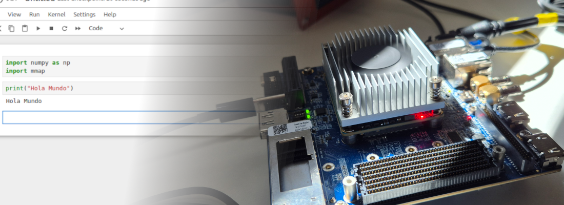
 TE0802
Since the early 90s, JTAG is the standard to program many different embedded devices like microcontrollers, processors and also FPGA. This standard is based on a serial protocol that allows the connection of different devices in a chain mode. JTAG is specially used in the debug step of a project, for example, when we are debugging the code that runs in an ARM processor, but then, when the product is finished, we usually store the program in a non-volatile memory like an SD card or an eMMC and the JTAG is not used again, since the processor can read from that memory and copy the corresponding code into de RAM. The case of the FPGA is not too different from processors. In this case, when the debugging time is finished, the design is stored in an external FLASH and then the FPGA boot reads that external FLASh and configures itself. In case of that FPGA is based on FLASH, like PolarFire or SmartFusion, the design is stored in the same chip.
Sometimes, and only sometimes, we will need to update the program, or the design once the product is delivered, In this case, if we are using a processor, we need to rewrite the program stored in the non-volatile memory, or simply change the SD card. In the case of an FPGA, we will need to update the content of the FLASH memory, and, what about a SOC? where we have an FPGA and an ARM processor. Focusing on AMD Zynq7000 and Zynq MPSOC, we need to know that the Processing System (PS) is the master in the boot process, so in case we need to update the firmware of the PS or the design of the Peripheral Logic (PL), will the PS who has to do it. To update the PS firmware, we will run the same steps ran to update the firmware of any other ARM, change the content of the non-volatile memory, but the case of the PL is different since we do have not a JTAG available to load the new design, will the PS who has to load the new design.
The PL of a Zynq7000 or Zynq MPSOC can be configured in three different ways.
- Using the JTAG.
- From the PL itself using the ICAP.
- From the PS using the PCAP.
Using the JTAG is the most common option. Using an external USB to JTAG adapter like the HS3 from Digilent we can configure the PL. Although this could seem the most simple method, it has some disadvantages. The first one is that the JTAG pins of the device have to be available, available for us, and available for everybody. If we create a board that is used in some sensitive project, allowing to anybody load any design in our board may be dangerous, for that reason, production SOMS like the ones designed by Trenz, or the Picozed do have not a JTAG connector (besides they can save some space of the board). So, although using the JTAG can be the easiest way to program the PL, sometimes it is not recommendable.
The second method is using the ICAP peripheral, which is located in the PL. This method is very useful when we have an FPGA instead of a SOC, so we can reconfigure the FPGA from the FPGA itself, but this means that we need to create the logic in the PL design to manage this, which is mandatory using an FPGA, but using a SOC, maybe is easiest execute all this logic in the processor. in my case, I use the ICAP when I need to load a new design in the QSPI memory, and then reconfigure the FPGA setting a specific address of the FLASH memory. Also, if you are working with soft-cores instead of hard-cores, this method will be the only one available for you. In this case, you can use the IP AXI_HWICAP
Last, we have the PCAP, which is similar to the ICAP, but managed by the PS, so we can use all the potential of the PS to receive, store one or more designs, and choose which design to load according to external or internal conditions. In this post, I am going to show you how we can do this on a Zynq MPSOC using the Trenz TE0802 board.
Creating a base PL design
First, we are going to create a base project in Vivado. To do that we need to add the Vivado installation folder to the path by executing the script settings64.sh, located in the Vivado installation path.
pablo@friday:~$ source /media/pablo/data_m2/xilinx/Vivado/2022.2/settings64.sh
pablo@friday:~$ vivado
Now, we are going to create a new project. The board I am going to use is the Trenz TE0802. We can download the board file from the Xilinx repository. To do that, in the project creation wizard, when it ask us about the part or board, we can search the TE0802, and then download the corresponding files. There are two different boards, each one with a different DDR manufacturer. In my case, I have the ISSI version, so it will be that which I have to select.

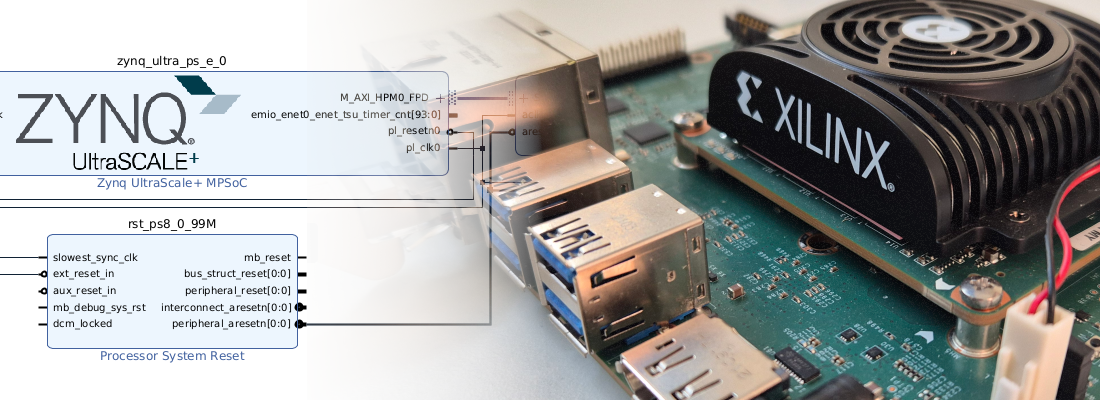
In the process I am going to follow, the board, or even the part used, is not relevant, since the process is the same for all Zynq 7000 and Zynq MPSOC. Once the project is created, we are going to create a block design. In this block design we need to think about what we will need in the ARM core in the future. I mean, we will be able to change the design which is loaded into the FPGA side, but at the same time, Petalinux will run within the PS, and this cannot be changed because the Petalinux distribution won’t change. So, for the sake of this project, I am going to enable a master AXI interface from the Low Power Domain (LPD), and I will let the two clocks that the board file enables for this board. The base block design will look like the next.

In this block design, there are a wire in the PL which is necessary for the AXI, so, when we create new designs for the PL, we need to ensure that this wire is still in the PL.
Once we have our base design, we can create the bitstream, and export the hardware in order to create the Petalinux distribution.
Building Petalinux
The next step is creating the Petalinux distribution. First, we need to add to the PATH the corresponding folder. To do that we can execute the script located in the Petalinux installation folder name settings.sh.
pablo@friday:~/workspace_local/te0802_ptlnx$ source /media/pablo/data_m2/xilinx/PetaLinux/2022.2/settings.sh
PetaLinux environment set to '/media/pablo/data_m2/xilinx/PetaLinux/2022.2'
WARNING: /bin/sh is not bash!
bash is PetaLinux recommended shell. Please set your default shell to bash.
WARNING: This is not a supported OS
INFO: Checking free disk space
INFO: Checking installed tools
INFO: Checking installed development libraries
INFO: Checking network and other services
WARNING: No tftp server found - please refer to "UG1144 2022.2 PetaLinux Tools Documentation Reference Guide" for its impact and solution
Now, as usual, we are going to create the project, that in my case is named os_te0802_ptlnx.
pablo@friday:~/workspace_local/te0802_ptlnx$ petalinux-create --type project --template zynqMP --name os_te0802_ptlnx
Next, navigate into the Petalinux project folder, and we are going to configure our distribution, as well as indicate the .xsa file generated by Vivado using the command petalinux-config.
pablo@friday:~/workspace_local/te0802_ptlnx/os_te0802_ptlnx$ petalinux-config --get-hw-description="../hw_te0802_ptlnx"
In this configurator, we need to enable the field FPGA Manager. This configuration will add some changes in the device-tree and the device-tree overlay, adding the PL as a new device. The configurator also allow us to specify a hardware directory path, but this is completely optional.

Only with this configuration, our Petalinux distribution will be able to configure and read the PL.
When Petalinux is configured, we can package all using the command petalinux-package.
pablo@friday:~/workspace_local/te0802_ptlnx/os_te0802_ptlnx/images/linux$ petalinux-package --boot --uboot
[INFO] Sourcing buildtools
INFO: Getting system flash information...
INFO: File in BOOT BIN: "/home/pablo/te0802_ptlnx/os_te0802_ptlnx/images/linux/zynqmp_fsbl.elf"
INFO: File in BOOT BIN: "/home/pablo/te0802_ptlnx/os_te0802_ptlnx/images/linux/pmufw.elf"
INFO: File in BOOT BIN: "/home/pablo/te0802_ptlnx/os_te0802_ptlnx/images/linux/bl31.elf"
INFO: File in BOOT BIN: "/home/pablo/te0802_ptlnx/os_te0802_ptlnx/images/linux/system.dtb"
INFO: File in BOOT BIN: "/home/pablo/te0802_ptlnx/os_te0802_ptlnx/images/linux/u-boot.elf"
INFO: Generating zynqmp binary package BOOT.BIN...


****** Xilinx Bootgen v2022.2
  **** Build date : Sep 26 2022-06:24:42
    ** Copyright 1986-2022 Xilinx, Inc. All Rights Reserved.


[INFO]   : Bootimage generated successfully

INFO: Binary is ready.
WARNING: Unable to access the TFTPBOOT folder /tftpboot!!!
WARNING: Skip file copy to TFTPBOOT folder!!!
Notice that the image generated before has not a .bit file loaded, so the design only uses the PS.
When the boot image is generated we can copy them with the root file system and the Linux kernel image to an SD card. The SD card has to contain two different partitions, one for the boot files, and the other one for the root file system. The partition where the boot is located has to be formatted using the FAT file system, and the partition for the root file system has to be EXT4. I have use the application disks to generate the partitions.

In the boot partition, we need to copy the boot.scr, BOOT.bin and image.ub files. On the other partition, we need to extract the content of the compressed file rootfs.tar.gz.
Now, it’s time to boot the board. When the SD card is inserted, we need to check the boot switches. In the TE0802 are located next to the VGA connector. The correct position for an SD card boot is the next.
| S1.1 | S1.2 | S1.3 | S1.4 |
|---|---|---|---|
| ON | ON | OFF | OFF |
Since the 2022 versions of Petalinux, the user root has no longer been available, and the petalinux user is used instead. The password for this user needs to be changed in the power-up of the board. This is important because we cannot connect to the board using SSH the first time. We will need to use the USB connection for the first login, and then, when the password is configured, we will be able to use SSH. Once the password has been set, we can use the ssh commnad to connect the board to the host computer. Maybe you are asking what is the reason to SSH connection instead of the USB, and that is because we will need to send to the board the new bistream, and this can be done easily using scp.
pablo@friday:~$ ssh [email protected]
When we are connected to the board, we can check the command fpgautil, which will be the command used to configure the PL. This command uses the PCAP to configure the PL, thus loading a partial bitstream (partial reconfiguration), loading the complete bitstream, loading a signed bitstream as well as reading the bitstream (readback), and reading the configuration.
oste0802ptlnx:~$ fpgautil -help

fpgautil: FPGA Utility for Loading/reading PL Configuration

Usage:	fpgautil -b <bin file path> -o <dtbo file path>

Options: -b <binfile>		(Bin file path)
         -o <dtbofile>		(DTBO file path)
         -f <flags>		Optional: <Bitstream type flags>
				   f := <Full | Partial >
         -n <Fpga region info>  FPGA Regions represent FPGA's
                                and partial reconfiguration
                                regions of FPGA's in the
                                Device Tree
				Default: <full>
	  -s <secure flags>	Optional: <Secure flags>
				   s := <AuthDDR | AuthOCM | EnUsrKey | EnDevKey | AuthEnUsrKeyDDR | AuthEnUsrKeyOCM | AuthEnDevKeyDDR | AuthEnDevKeyOCM>
	  -k <AesKey>		Optional: <AES User Key>
	  -r <Readback> 	Optional: <file name>
				Default: By default Read back contents will be stored in readback.bin file
	  -t			Optional: <Readback Type>
				   0 - Configuration Register readback
				   1 - Configuration Data Frames readback
				Default: 0 (Configuration register readback)
	  -R 			Optional: Remove overlay from a live tree

Examples:
(Load Full bitstream using Overlay)
fpgautil -b top.bit.bin -o can.dtbo -f Full -n full
(Load Partial bitstream using Overlay)
fpgautil -b rm0.bit.bin -o rm0.dtbo -f Partial -n PR0
(Load Full bitstream using sysfs interface)
fpgautil -b top.bit.bin -f Full
(Load Partial bitstream using sysfs interface)
fpgautil -b rm0.bit.bin -f Partial
(Load Authenticated bitstream through the sysfs interface)
fpgautil -b top.bit.bin -f Full -s AuthDDR
(Load Parital Encrypted Userkey bitstream using Overlay)
fpgautil -b top.bit.bin -o pl.dtbo -f Partial -s EnUsrKey -k <32byte key value>
(Read PL Configuration Registers)
fpgautil -b top.bit.bin -r
(Remove Partial Overlay)
fpgautil -R -n PR0
(Remove Full Overlay)
fpgautil -R -n full
Note: fpgautil -R is responsible for only removing the dtbo file from the livetree. it will not remove the PL logic from the FPGA region.
Generating a new PL design
The next step is generating a new bitstream, making some changes on the PL side.
I have added to the block design a counter that is connected to the LEDs of the board. The design is so simple but it will be valid to verify that the new bitstream is configured.

When the block design is complete, before generate the bitstream we have to make a change in the project settings. The file we need to pass to the fpgautil application has to be a binary file, that is with the .bin extension. By default, the bitstream is generated only with the .bit extension. To generate also the binary file we need to configure the implementation process to do it.

Now we can generate the bitstream, and two different files will be generated. Then, the binary file has to be sent to the board using scp.
pablo@friday:~/workspace_local/te0802_ptlnx/hw_te0802_ptlnx/hw_te0802_ptlnx.runs/impl_1$ scp ./hw_te0802_ptlnx_bd_wrapper_2.bin [email protected]:.
Configuring the new design
When the file is sent to the board, we can use fpgautil to configure the PL. Since this application has to make some changes in privileged folders, we needs to execute it using sudo, and introducing the password.
oste0802ptlnx:~$ sudo fpgautil -b hw_te0802_ptlnx_bd_wrapper.bin -f Full

We trust you have received the usual lecture from the local System
Administrator. It usually boils down to these three things:

    #1) Respect the privacy of others.
    #2) Think before you type.
    #3) With great power comes great responsibility.

Password:
Time taken to load BIN is 174.000000 Milli Seconds
BIN FILE loaded through FPGA manager successfully
When the process is complete, the new bitstream will be configured in the PL, and the output of the counter will be visualized in the eight LEDs of the board.
What we have seen in this post has incredible potential. Using a SOC based on Processor+FPGA not only you can implement some custom peripherals in the PL, but you can even change these peripherals according to external configurations received by Ethernet, WIFI or any other interface. You will be able to change the entire functionality of your device only sending a new configuration, isn’t it great? With this kind of functionality, the potential of the FPGA is multiplied, multiplied exactly by the different designs that can be stored in an SD card.