Implementing a dual core processor in FPGA.
A few years ago, microprocessors manufacturers competed to get the fastest processor. High speed means more tasks can be executed in the same amount of time, but also, means higher power consumption. To improve this, the voltages of the core start decreasing to levels below 1V, and according to the equation P=VxI, the power will be decreased as well, but decreasing the voltage is not the solution to all their problems, because as the voltage decrease, the transistors in the processors turns slower, so what we solve on the one hand, we make it worse on the other. At this point, the manufacturers arrived a compromise between speed and voltage, and I am not sure if there was any processor above 5GHz. To keep improving the performance of the processors, manufacturers starts to integrate in the same part more than one processor, at the beginning with many shared parts, but now we can find several complete processors in the same part that can work together or separately execute different tasks or even different operating systems. Multi-core fever is not only for high-end processors, there are many “little” microprocessors or even microcontroller families that offer 2 or more cores with very competitive prices.
At this point, we have seen the advantages of multi-core systems, and in this blog, we already use them when we use Zynq7000 family (Arm A9 dual-core processor), and Zynq MPSOC family (Arm A53 Quad-core processor + Arm R5 dual-core processor). These two examples are perfect to explain the big difference between them. Both are multi-core systems, but Zynq7000 has 2 similar cores, with the same characteristics, benefits and limitations, on the other side, Zynq MPSOC has 2 different kinds of processors, and each one is complemented with the other one since they have different capabilities. Now, what about FPGAs? well, FPGAs are a blank canvas, and we can implement a customizable multi-core system, even in little FPGA. In this post, I will show you how we can implement in the Digilent’s Arty A35 board a dual-core system, with one core processor dedicated to communications, run a real-time Operating System (RTOS), and manage the main IOs. This core will act as the main core. The other one will be used as a mathematical co-processor, with floating point capabilities, and fast memory access.
First, we will open Vivado and we have to create a new project for the Digilent Arty A35T board (board file available here). This board is based on Artix 7 A35T, an FPGA with 33k logic cells. For this kind of project, we also need to verify the amount of Block RAM available, since this memory will be used as local memory for the co-processor. In this part, we have a total of 1.8 Mb of BRAM, which is enough for this project. Also, in the Arty board, we can find 256Mb of DDR3 RAM that we will use to store the application of the main core, several LEDs and buttons, and many IOs. Once the project is created we will create a block design. Now on the left of the block design, we can find a tab named Board. In this tab, we can find the HW elements that we can find on the board. First, we will add the clock. Now by double-clicking on the IP we can configure it. The first tab is the interface with the board, and we can see how the input CLK_IN1 is connected to the signal sys_clock, which is configured by default.
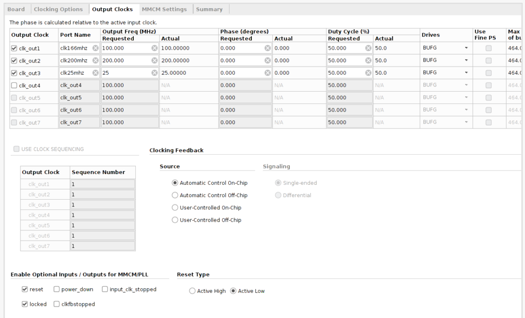
In the Output Clocks tab, we will configure the needed clocks for the design. Since we will use the external DDR3 RAM, we need to include in our design a MIG. This IP needs a 200MHz clock, and a 166Mhz clock for the Arty board. Also we will need a 25Mhz clock for the Ethernet phytter. IN this tab, we also need to configure the Reset Type as Active Low.
Now we can add the Memory Interface Generator. inputs clk_ref_i and sys_clk_i are connected to an external ports by default. We need to delete the external ports and connect the input clk_ref_i to 200MHz clock, and the input sys_clk_i to the 166Mhz clock.
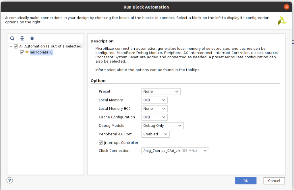
Now we can add the first Microblaze processor. Clicking in Run Block Automation, we will select the Microcontroller preset, and the rest of the options will remain by default.
The button Run block automation will be enabled again, this time to configure the ports and memories of the Microblaze. Local memory size for the main processor has no importance since the code will run in the external memory but is interesting to keep enabled the local memory because it is faster than the external, and maybe we will need to execute some tasks faster than others, so an 8 kB of memory should be enough. The clock has to be connected to the output clock of the MIG module since the processor needs to be synchronized with this clock to enable communication to read the instructions and write data.
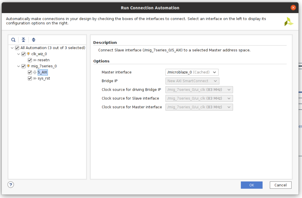
At this point, we will have our Microblaze configured with the basic connections. Now we have to connect the AXI interface to enable the RAM memory. reset ports will be connected to the external reset automatically. AXI connection of the MIG can be connected to the Cached port or to the peripherals port. The cached port includes a cache memory that improves performance and is very interesting when we are using external memories.
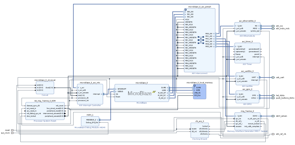
Now we will add the rest of the peripherals starting by the Ethernet MII, which will need to make external the 25Mhz clock. Also, we will add from the board tab the USB UART, LEDs and Push Buttons. All of them are connected to the Peripheral AXI and the ui_clk. Also, we will add an AXI Timer that will be used for the RTOS. The entire block design for the main core is shown in the next image.
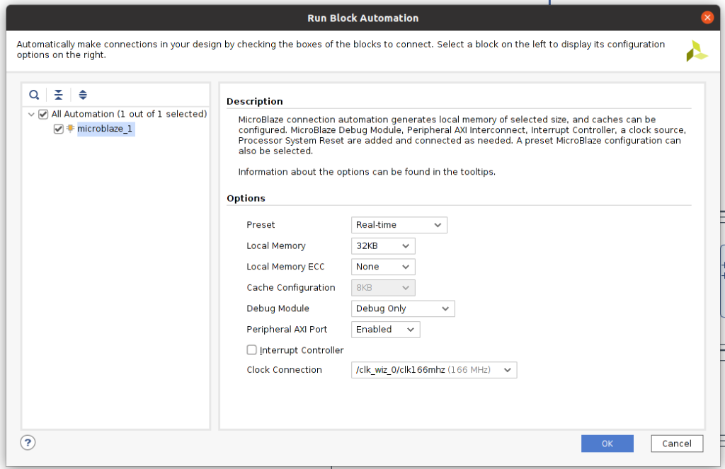
Now is the time for the co-processor. We need to add a second Microblaze to the block design. This time we will change the default presets. First, we need to apply the Real-time preset. Also, since this processor has no access to the external RAM memory, we are going to increase the local memory up to 32kB. Remember that this processor is only to perform some mathematical operations, so the amount of code will be low. Also, we will disable the interrupt controller, and the clock will be connected to 166 MHz to improve the performance.
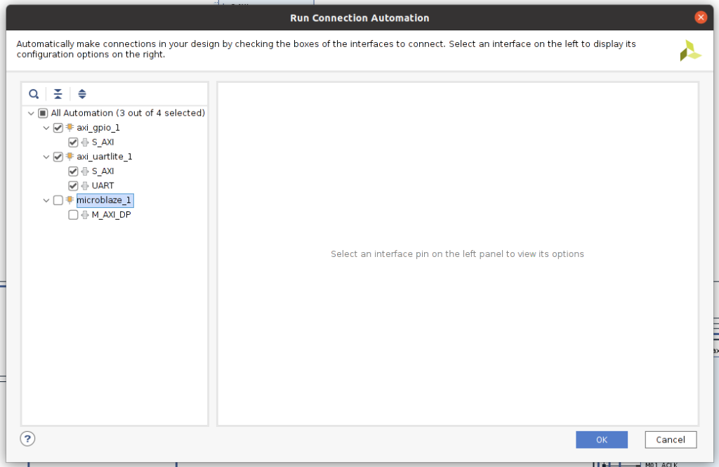
In the configuration of the second processor, we will disable the Data and Instructions cache and we will enable the Floating Point Unit. For now, we don’t open the Run Connection Automation. First, we will add the peripherals that this processor will access. We need to include in the block design the RGB LEDs of the board and the switches. Also, we will add a second Uart Lite IP to debug this second processor. Now we can click over Run connection automation and connect all of these peripherals to the AXI port of the Microblaze 1 and the 166MHz clock. We will keep unselecting the AXI port of the Microblaze_1 since the only options available are the peripherals of the microblaze_0. This port will be automatically connected when we connect the rest of the peripherals to the microblaze_1 AXI peripheral.
Now we have a block design with 2 MicroBlaze processors that can run independently, but we need a way to communicate them. There are some methods to communicate both peripherals, and we will use shared memory with separate regions for write and reading. To do that we will add an AXI Bram Controller, and configure it with only one BRAM interface. Now we can connect the AXI port to the microblaze_0 AXI port by clicking on Run connection automation. The BRAM block created has only one interface, we need to change this in the configuration of the BRAM block by configuring the Memory Type as True Dual Port RAM. Now we will add a second AXI BRAM controller, again with only 1 BRAM interface, and we will connect this one to the AXI interface of the microblaze_1, and the BRAM port to the second port of the BRAM added before. This way both processors have access to this memory.
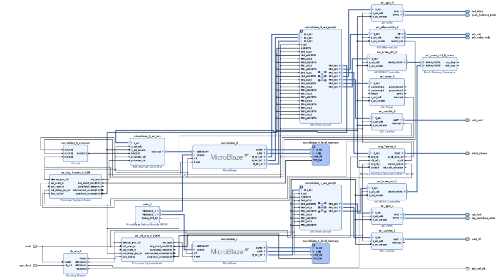
The entire block design is shown in the next figure.
Finally, we can generate the wrapper of the block design.
Now we have to define the constraints for the ports that are not configured by default, which are the 25 MHz ethernet reference clock, and the second UART for the co-processor connected to the PMOD A.
set_property PACKAGE_PIN G18 [get_ports eth_ref_clk]
set_property IOSTANDARD LVCMOS33 [get_ports eth_ref_clk]

set_property PACKAGE_PIN G13 [get_ports uart_rtl_txd]
set_property IOSTANDARD LVCMOS33 [get_ports uart_rtl_txd]

set_property PACKAGE_PIN B11 [get_ports uart_rtl_rxd]
set_property IOSTANDARD LVCMOS33 [get_ports uart_rtl_rxd]
Now we can generate the bitstream, and then export the hardware including the bitstream.
Once the hardware is exported, we have to open Vitis from Tools > Launch Vitis IDE.
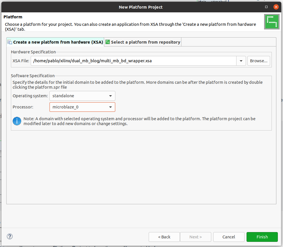
Inside Vitis we will create a new Platform Project to from the .xsa file created before. In the platform creation wizard, only one processor can be included, so we will include the microblaze_0.
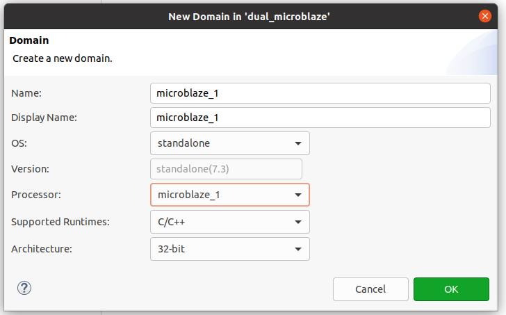
Once the platform is created, we can add a new domain for the microblaze_1 processor.
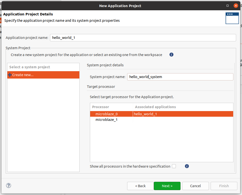
Now we have a platform with 2 different processors, The next is to create an application project for the first Microblaze, using the template Hello World. The name will be hello_world_1, and also we will create a system named hello_world_system. In this system, we will create the application for both processors, and then we will debug the entire system.
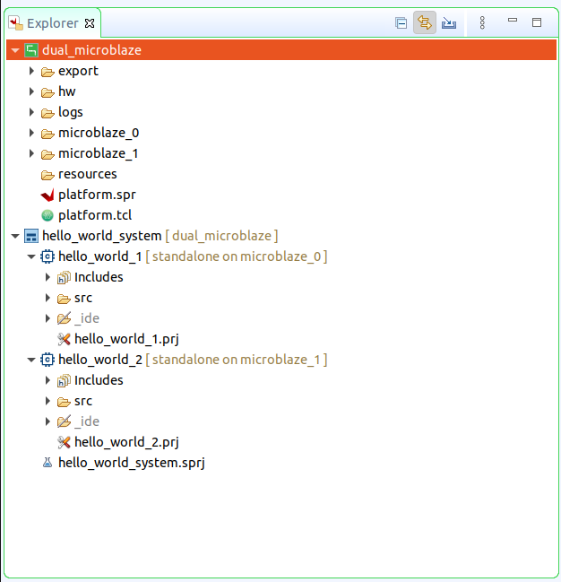
Once the project for the microblaze_0 is created, we will do the same for the microblaze_1, using the same system. The final project tree is the next.
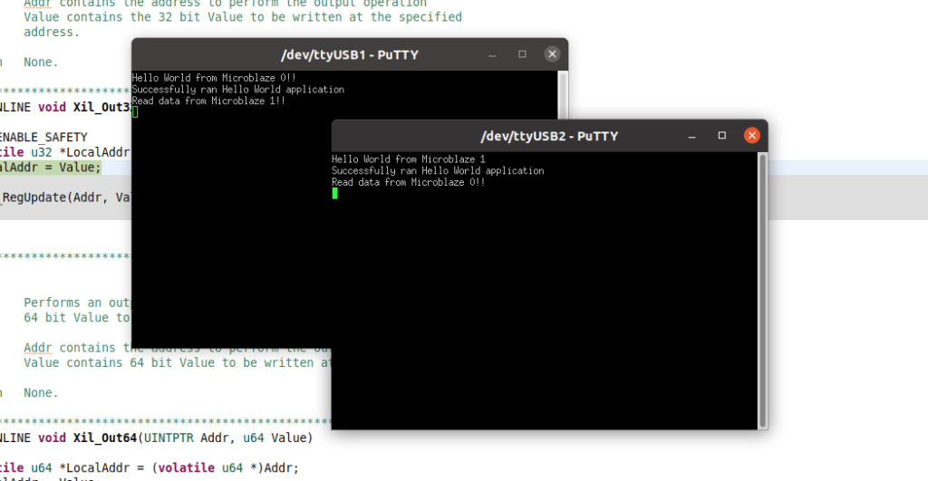
When both projects are created we are going to modify the template. The goal will be that both processors send a message through UART, and then MicroBlaze 1 writes a word in the first half of the shared memory, and read a word in the second half of the shared memory. On the other side, the microblaze_1 will send a message through its UART, which is connected to PMOD_A, and then write a word in the second half of the shared memory and read a word in the first half of the shared memory.
The code for the microblaze_0 is the next.
#include <stdio.h>
#include "platform.h"
#include "xil_printf.h"
#include "xil_io.h"

#define SHARE_WRITE_MB0_BASE XPAR_AXI_BRAM_CTRL_0_S_AXI_BASEADDR
#define SHARE_WRITE_MB0_END (XPAR_AXI_BRAM_CTRL_0_S_AXI_BASEADDR + 0x000007ffU)
#define SHARE_READ_MB0_BASE (XPAR_AXI_BRAM_CTRL_0_S_AXI_BASEADDR + 0x00000800U)
#define SHARE_READ_MB0_END XPAR_AXI_BRAM_CTRL_0_S_AXI_HIGHADDR

int main()
{
    init_platform();

    print("Hello World from Microblaze 0!!\n\r");
    print("Successfully ran Hello World application \n\r");

    Xil_Out32(SHARE_WRITE_MB0_BASE, 0x00003434);

    while(Xil_In32(SHARE_READ_MB0_BASE) != 0x00004545);
    print("Read data from Microblaze 1!!\n\r");
    cleanup_platform();
    return 0;
}
And the code for the microblaze_1, with read and write addresses flipped is the next.
#include <stdio.h>
#include "platform.h"
#include "xil_printf.h"
#include "xil_io.h"

#define SHARE_WRITE_MB1_BASE (0xC0000000 + 0x00000800U)
#define SHARE_WRITE_MB1_END 0xC0000fff
#define SHARE_READ_MB1_BASE 0xC0000000
#define SHARE_READ_MB1_END (0xC0000000 + 0x000007ffU)

int main()
{
    init_platform();

    print("Hello World from Microblaze 1\n\r");
    print("Successfully ran Hello World application \n\r");

    Xil_Out32(SHARE_WRITE_MB1_BASE, 0x00004545);

    while(Xil_In32(SHARE_READ_MB1_BASE) != 0x00003434);
    print("Read data from Microblaze 0!!\n\r");
    cleanup_platform();
    return 0;
}
The outputs in two putty terminals are shown in the next capture.
At this point, we have a heterogeneous dual-core system with a main processor that will be in charge of managing the tasks and the communications and a second fastest processor with floating point capabilities. besides these 2 processors, remember that both Microblaze has AXI interface, so we can add hardware accelerators for specific tasks like HASH computing or xFFT.


