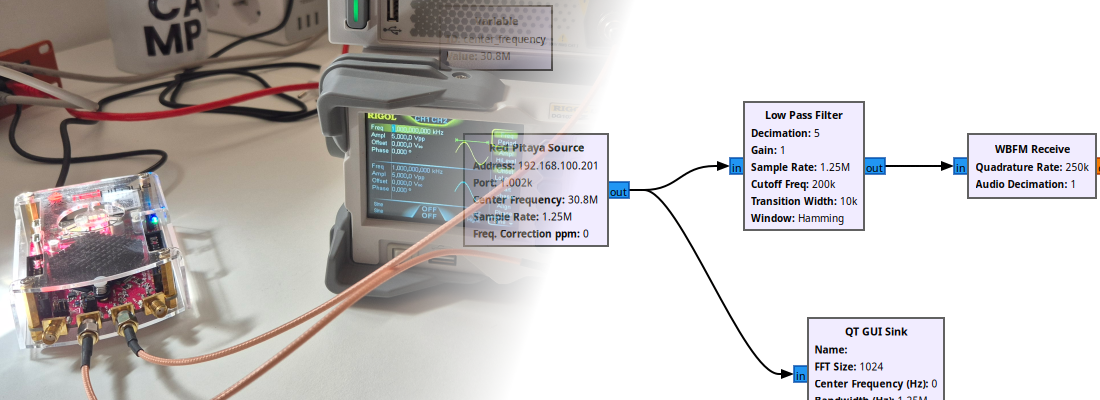
Using DSP48E1 Slice.
A few years ago, FPGAs were used almost exclusively for communication systems. On the other hand, DSPs are used to execute digital signal processing algorithms. The reason is the hardware components that were integrated. FPGAs, were based on flip-flops, LUTs and general logic, unlike DSP which was based on a general purpose microcontroller, with dedicated hardware to perform multiplications and accumulations (MACC) in a very efficient way. Nowadays, FPGAs are often used in signal processing and the reason of that is the integration inside the same part, the high speed logic, and MACC modules.
Xilinx’s devices have inside multiple types of slices, for general purpose (SliceL), memory (SliceM),… and to perform MAC operations, the DSP48E1 for 7 series, and DSP48E2 for Ultrascale. On this post, I am going to focus on DSP48E1, but is valid for the DSP48E2, except for the widths, which are different.
The structure of the DSP48E1 can be found on the next image. We can see that the slice has many ports, but they can split in 2 groups. A, B, C, D and P are operands and the result ports, and the rest of the ports, both inputs and output are for control.

Essentially, the operation performed by this slice is P = (A+D)*B+C. Regarding the widths, input A has a width of 30 bits, input B has a width of 18 bits, input C has a width of 48 bits, and input D has a width of 25. The slice has a pre adder where the values on A and D are added. Is important to notice that, despite of the width of A is 30, pre adder output has 25 bits, and this output is connected to the 25 operand input for the multiplier. The other multiplier input has the same size as the B input, 18 bits. At this point, we know that the multiplier can perform multiplications up to 25×18 bits. The second part of the Slice is very configurable, and can perform additions, subtractions or patterns detection. The function that is important for us is the addition, because thanks to this, we can implement FIR cells in only one slice.
In general, if we want to perform any operation on an FPGA, we only have to write the corresponding code in VHDL or Verilog, and the synthesizer will translate this code in the correct combination of the elements of the FPGA. The case of the multiplications is not totally an exception, and we can infer a DSP48E1 slice only by the symbol *. The next code is an example.
module test_dsp48e1 #(
  parameter width_a = 16,
  parameter width_b = 16,
  parameter width_c = 32
  )(
  input clk,
  input rstn,

  input [width_a-1:0] a,
  input [width_b-1:0] b,
  input [width_c-1:0] c,

  output [width_a+width_b-1:0] r
);

  reg [width_a-1:0] reg_a;
  reg [width_b-1:0] reg_b;
  reg [width_c-1:0] reg_c;

  assign r = (a*b)+c;

endmodule
This code is synthesized with only 1 DSP slice. Notice that the width of a and b are lower than 18 bits, and this is important. In case of only one of the operands in the multiplier is greater than 18, the thing changes. If we synthesize the same code, with the next widths,
parameter width_a = 18,
parameter width_b = 19,
parameter width_c = 37
We can see that the multiplication is inferred in one DSP48E1 slice, but the addition is inferred with logic.

Regarding how the slice perform the operation, DSP48E1 slice give us the choice to use its internal registers, without infer them on other slices.

Each pre-adder has inside several registers that can be bypassed with the control input INMODE. Inferring the operation with ‘*’ symbol, we let the synthesizer the decision to use this registers or not, and, in general, the synthesizer selection will be good for our design, but if you want to have a exhaust control of the resources, or the delay, the best way yo get this is configure the slice manually, or at least, say to the synthesizer what we want.
The way to configure the DSP48E1 manually, is defined on UG953. Using this definition of the macro, we will have absolute control over the behavior of the slice, but, as you can see, there are a lot of control inputs to configure, and the possibilities to make some wrong are high.
Exist a mid point between inferring and instantiate, and for me, is the best option, use the language templates. On Vivado, under the Flow Navigator, you have a link to open Language Templates. On the window opened, under Device Macro Instantiation, selecting the correct family, you can see a folder with the name DSP48. For the example we had used, we have to open the template Multiply Accumulate (MACC). The same code example with the extended width, using template, will looks like this.
module test_dsp48e1 #(
 parameter width_a = 19,
 parameter width_b = 18,
 parameter width_c = 37
 )(
 input clk,
 input rstn,

 input [width_a-1:0] a,
 input [width_b-1:0] b,
 input [width_c-1:0] c,

 output [width_a+width_b-1:0] r
 );

   MACC_MACRO #(
      .DEVICE("7SERIES"), // Target Device: "7SERIES"
      .LATENCY(3),        // Desired clock cycle latency, 1-4
      .WIDTH_A(19),       // Multiplier A-input bus width, 1-25
      .WIDTH_B(18),       // Multiplier B-input bus width, 1-18
      .WIDTH_P(37)        // Accumulator output bus width, 1-48
   ) MACC_MACRO_inst (
      .P(r),  // MACC output bus, width determined by WIDTH_P parameter
      .A(a),  // MACC input A bus, width determined by WIDTH_A parameter
      .ADDSUB(1'b1), // 1-bit add/sub input, high selects add, low selects subtract
      .B(b),  // MACC input B bus, width determined by WIDTH_B parameter
      .CARRYIN(1'b0), // 1-bit carry-in input to accumulator
      .CE(1'b1),     // 1-bit active high input clock enable
      .CLK(clk),   // 1-bit positive edge clock input
      .LOAD(1'b1), // 1-bit active high input load accumulator enable
      .LOAD_DATA(c), // Load accumulator input data, width determined by WIDTH_P parameter
      .RST(!rstn)    // 1-bit input active high reset
   );
endmodule
In this case, the result of the operation is the same, but before, the result of the synthesis had perform the accumulation out of the slice. In this case, the result is the next.

Despite of the zoom, we can see that the entire operation is implemented by only one slice.
In case of the Ultrascale Slice, the DSP48E2, the multiplicator operands width is increased to 18×27, which will allow us reduce the number of slices in case of greater operations.
Language templates is a very useful resource when we want to ensure that the code we have wrote, will be understood by the synthesizer correctly. DSP48E1 is only an example of all the templates that we have. The example I propose you is an example that can be integrate in any type of filter FIR or even IIR, and the way Y show you is the best to ensure a good resources optimization, with a easy implementation.