Emulating hardware with Zynq.
Due to quarantine, most of us are working from home, and seems that the way we used to work, even more when our work consist in write or develop with our laptop, will be change. When your work is computer based, for example, on web, is easy still working from home with the same benefits and limitations that you have in the office, maybe the coffee with your job mate will be different because honestly, humans are sociable beings, and although there are tools for try to improve our work relations, like Microsoft Teams, this coffee tastes very different, sometimes better due to the coffee machines of the office.
Other kind of jobs, may be computer based too, but, for example, in my case, when I finish the development, I have to test it in a power electronics equipment, and bring one of this devices to my home may be very difficult due to the dimensions of it, and also very dangerous begause the voltage and current levels that I need to test my design correctly, so is necessary an engineer that test my design in the laboratory. The fact that I can not test my desing, does that the design I sent to the test engineer are less tested than if I could test it for myself. and this may delay the release date.
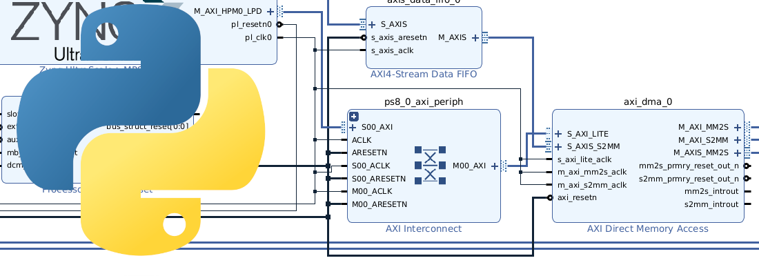
At this point, we can ask ourselves, what we have in home for test our design, and improve our work. Well, in my case, I have a development board with the same fpga that I use in my work, so the only I need for still working is the power electronics device that my design have to control. Due to the reasons mentioned before, that’s not possible but, I can emulate the response of the device that I have to control, without need of the device himself, and that’s will be the role of Zynq, Pynq and the analog output board for Pynq-Z2.
The real design, is formed by a control board, and the power electronic stage. The control board receive the analog measures from the power electronics stage, and send the pwm signals to the control board, so our emulator will send analog signals to the control board and receive pwm signals from the control board. That will be the mission of the Analog Output board that I’ve design.

This board has 16 analog outputs from -15 to +15 volts, with up to 20mA each one. The board is stackable, getting up to 48 analog outputs. Each board has 3 digital input/output. With this board we have the interfaces solved, next, emulate the behavior of the power stage.
The behavior of the power stage will be defined as the analog output value according the digital inputs. Luckily, the behavior of almost everything will be defined by mathematics, and the power stages is not different. Regarding the complexity of the model, we can obtain more accurately behavior, or more variables to control. As an example of that, I’ve prepared an example of a SMPS Buck. There are several models of the Buck power supply according the control that we will use. In this case I will use the model for output voltage, that consists is emulate the output LC filter. For obtain the discrete equation I use the next Octave script.
clear all

pkg load control

s = tf('s');

fs = 1e6;
L = 660e-6;
C = 600e-6;
RC = 1e-4;
R = 1;
vin = 24;
vref = 6;

## LC filter definition
h = 1/(L*C)*(s*RC*C+1)/(s^2+s*1/(R*C)+1/(L*C));

## Discretize system
hz = c2d(h,1/fs)

step(hz)

[num,den]=tfdata(hz);

## (Az^2+Bz+C)/(z^2+D*z+E)
A = num{1}(1)
B = num{1}(1)
C = num{1}(2)
D = den{1}(2)
E = den{1}(3)

## Quantification
nbits = 30;
Aq = floor(A*2^(nbits))
Bq = floor(B*2^(nbits))
Cq = floor(C*2^(nbits))
Dq = floor(D*2^(nbits))
Eq = floor(E*2^(nbits))
Once we have the constants for our model computed, we have to implement it in the FPGA and this will be our buck model. This model, in my case is computed at 1MHz. This maximum speed will depend of the design. Even executing model at 1MHz, the Analog Output board max speed is 100kHz, but for this kind of model, this is not a limitation because the output voltage max frequency sure is less than 100kHz. For test the model, I’ve made a step response, and this is the result.

I will use an Arty board for implement the control of the Buck power supply, and the XADC for acquire signals. The control implemented in Arty is an Hysteresis control, that will give us at the output a little ripple. For the test, I’ve changed the input voltage and the output voltage must remain at the same voltage around 1,2 volts.


For this example I used only 1 output of the 16 available, but imagine a design with several measures like and three phase grid inverter, where we could have 3 AC voltage measures, at least 1 DC voltage measure, 3 AC current measures and 1 DC current measure, and all of them multiply by the number of power stages to control.
Hope you find this post interesting.