DDR Resources

When most of us hear DDR, the first think that comes to our mind is RAM memories, but DDR is related with the comunication protocol, not with the memory. DDR means Double (Dual), Data Rate. This, basically means that un 1 single clock cycle, 2 data will be sended for every line. In this post I will show you how Xilinx FPGA manage DDR signals, and how make a design that communicates with a DDR device.
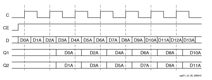
If we take a look to the UG471 of Xilinx, we can read that DDR input, and output are a configuration of OLOGIC, in clase of ODDR primitive, and ILOGIC, in case of IDDR primitive. DDR primitives has a simple configuration. The output is feed from 2 registers, one of them clocked with the input clock, and the second one clocked with the negate of the input clock.
ODDR
ODDR primitive is simple, it has 2 inputs for data, D1 for positive edge and D2 for negative edge, Set and Reset inputs, Clock enable and Clock. This primitive can be configured through 3 parameters: DDR_CLK_EDGE, where we can select when data is captured by the primitive. This parameter can take 2 values, SAME_EDGE or OPOSITE_EDGE, and although OPOSITE_EDGE is the default configuration, SAME_EDGE is more efficient, because input data is captured only in the rising edge of the clock, on the other hand, OPOSITE_EDGE capture input data in both rise and falling, and this add some logic to primitive. The second parameter is INIT, for select the initial value of Q, and finally SRTYPE, where we can select if Reset and Set signals are synchronous or asynchronous.

IDDR
IDDR, like ODDR, are a configuration for the ILOGIC blocks. ILOGIC blocks are a bit more sophisticated than OLOGIC but their operation is similar. IDDR blocks has 2 data outputs Q1 for positive edge, and Q2 for data received in the negative edge. Set an Reset inputs, clock enable and clock. Data is output through the D output. There are also 3 parameters for configure the IDDR primitive: DDR_CLK_EDGE in this case has 3 possible values, SAME_EDGE where data is presented in the rising edge of clock, SAME_EDGE_PIPELINED, that works similar to the SAME_EDGE, but add a clock delay for the first data, doing 2 first input data appear in the first rising edge, and OPOSITE_EDGE, where data is given in the edge where it arrives. Like the ODDR, the most efficient configuration is SAME_EDGE. Also, IDDR has a SRTYPE parameter and 2 for the initial state of the outputs Q1 and Q2.

Clock forwarding
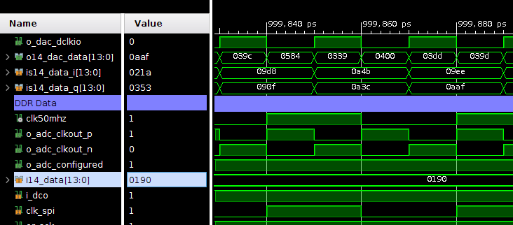
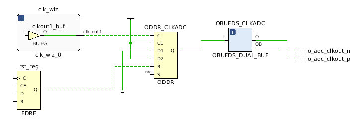
Regarding DDR primitives, I want to explain the clock forwarding technic. Many times, an external device like ADCs or DACs, need a clock signal, and this clock signal have to be synchronized with data signals, and in this case, the only way to satisfy that, is generate the clock signal on FPGA. When synchronization between clock and data is required, minimization of delays is mandatory, overall in clock signal. For avoid jitter in clock signal, is necessary clock paths from the clock origin, to the end. For ensure that FPGA use its clock resources up to the output pin ODDR primitives are the best solution. For do that, we only have to connect D1 input to “high”, and D2 output with “low”, and feeding the clock input with the desired output clock, we will have in the pin connected to Q output the desired clock with the minimum delay.

If our device need a differential clock, we only have to connect the Q output to an OBUFDS and ensure that the output pins of the OBUFDS are a differential pair. In the next code block, can see an example of clock forwarding for single-ended and differential clock.
/* Clock forwarding for DAC. Single anded clock */
ODDR #(
.DDR_CLK_EDGE("SAME_EDGE"),
.INIT(1'b0),
.SRTYPE("SYNC")
)ODDR_CLKDAC(
.Q(o_dac_clkout),
.C(clk100mhz),
.CE(1'b1),
.D1(1'b0),
.D2(1'b1),
.R(rst),
.S(1'b0)
);

/* Clock forwarding for ADC. Differential clock */
ODDR #(
.DDR_CLK_EDGE("SAME_EDGE"),
.INIT(1'b0),
.SRTYPE("SYNC")
)ODDR_CLKADC(
.Q(clk50mhz_ddr),
.C(clk50mhz),
.CE(1'b1),
.D1(1'b0),
.D2(1'b1),
.R(rst),
.S(1'b0)
);

OBUFDS #(
.IOSTANDARD("DEFAULT"),
.SLEW("SLOW")
) OBUFDS_CLKADC (
.O(o_adc_clkout_p),
.OB(o_adc_clkout_n),
.I(clk50mhz_ddr)
);

