Getting Started with the Forgix Board: Efinix Trion T8 + RP2350
 Forgix board
A few weeks ago, Adiuvo Engineering and Training released the Forgix board, a (very) small Teensy 4.0 form-factor board that pairs an Efinix Trion T8 FPGA with a Raspberry Pi RP2350. It is not the first board that features the great combo of a small FPGA and an RPxx, actually in this blog I show you the Cryptolite ICE, that features an ICE40 and an RP2040, or the Astria also from Adiuvo Engineering, that features a Spartan7 and an RP2040. Actually, and this is a bit offtopic, a few days ago I asked on X if the RPxxxx microcontrollers are used in production, and the reality is that they have even been sent to space! But today, unfortunately, we are not going to send anything to space — instead, we are going to talk about the Forgix board and how to get started with it.
Table of contents
- The Forgix board
- FPGA configuration
- Programming tools
- Interfacing the RP2350 with the FPGA
- Headless builds with Efinity
- Three examples to get started
- Conclusions
The Forgix board
The Forgix is designed by Adiuvo Engineering and Training together with American Embedded, and it follows the Teensy 4.0 pinout: two 14-pin side headers with 24 digital pins, 3V3, VIN, GND and a rear pad group (3V3 · VBAT · PROGRAM · ON/OFF · GND). Power comes from USB-C or VIN, with a TPS62162 buck feeding the 3.3 V I/O rail and a TPS7A20 LDO generating the Trion’s +1V1 core rail on-board.
Of the 24 header pins, six (0, 1, 2, 3, 4, 5) go to the RP2350 itself — pins 0/1 are one of its two hardware UARTs, 2/3 are plain GPIOs, 4/5 are the other hardware UART — and the remaining eighteen are routed straight to the Trion T8 fabric. That is a generous fraction of the FPGA’s I/O exposed directly on a Teensy-shaped header, which is the whole point of the board: a small, breadboard-friendly FPGA you can drop into an existing Teensy-based project.
You can find the full pinout in the table below
| Teensy pin | Net | Goes to | Signal / function |
|---|---|---|---|
| 0 | RP.UART1_RX |
RP2350 GPIO8 |
UART1 RX |
| 1 | RP.UART1_TX |
RP2350 GPIO9 |
UART1 TX |
| 2 | PIN2 |
RP2350 GPIO22 |
RP2350 GPIO (header break-out) |
| 3 | PIN3 |
RP2350 GPIO23 |
RP2350 GPIO (header break-out) |
| 4 | PIN4 |
T8 A5 |
FPGA GPIO (GPIOR_05) |
| 5 | PIN5 |
T8 D7 |
FPGA GPIO (GPIOR_17_CTRL6) |
| 6 | PIN6 |
T8 C7 |
FPGA GPIO (GPIOR_16_CTRL7) |
| 7 | RP.UART0_TX |
RP2350 GPIO12 |
UART0 TX |
| 8 | RP.UART0_RX |
RP2350 GPIO13 |
UART0 RX |
| 9 | PIN9 |
T8 D6 |
FPGA GPIO (GPIOR_15_CBUS0) |
| 10 | PIN10 |
T8 G7 |
FPGA GPIO (GPIOR_37_TEST) |
| 11 | PIN11 |
T8 G5 |
FPGA GPIO (GPIOR_34_CSI) |
| 12 | PIN12 |
T8 G2 |
FPGA GPIO (GPIOL_03_CDI4) |
| 13 | PIN13 |
T8 F5 |
FPGA GPIO (GPIOR_24) |
| 14 | PIN14 |
T8 F6 |
FPGA GPIO (GPIOR_26_CBSEL0) |
| 15 | PIN15 |
T8 E5 |
FPGA GPIO (GPIOR_23_CTRL4) |
| 16 | PIN16 |
T8 C6 |
FPGA GPIO (GPIOR_13) |
| 17 | PIN17 |
T8 B3 |
FPGA GPIO (GPIOL_16_CLK2) |
| 18 | PIN18 |
T8 B7 |
FPGA GPIO (GPIOR_10) |
| 19 | PIN19 |
T8 A7 |
FPGA GPIO (GPIOR_07) |
| 20 | PIN20 |
T8 A3 |
FPGA GPIO (GPIOL_18_CTRL2) |
| 21 | PIN21 |
T8 C2 |
FPGA GPIO (GPIOL_12_CTRL0) |
| 22 | PIN22 |
T8 D2 |
FPGA GPIO (GPIOL_11_CDI3) |
| 23 | PIN23 |
T8 E2 |
FPGA GPIO (GPIOL_09_CDI2) |
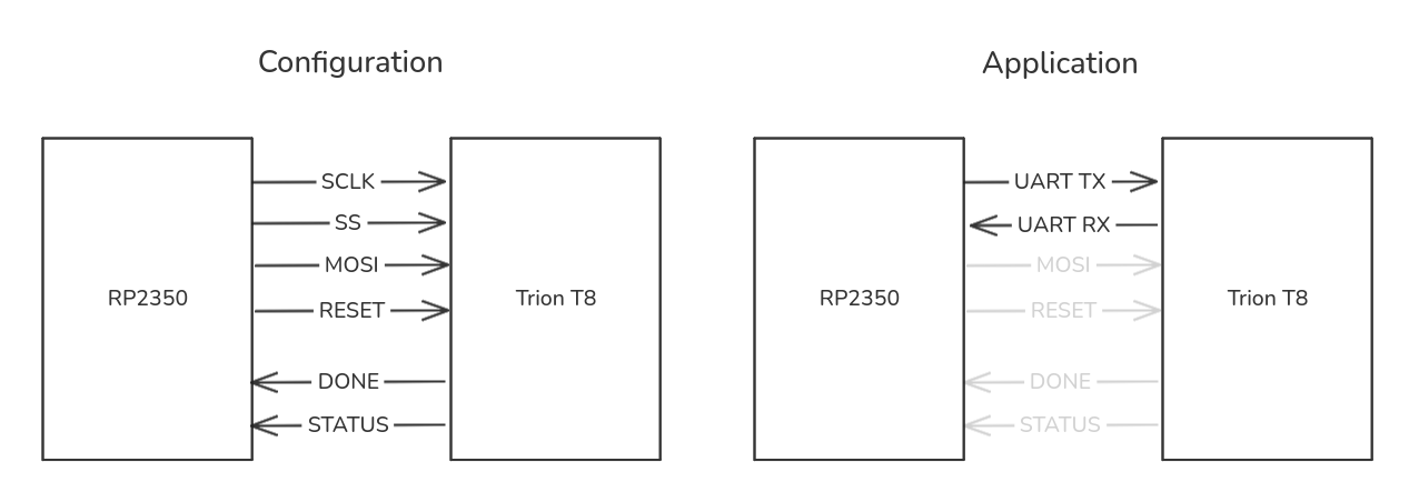
FPGA configuration
The Trion T8 has no volatile configuration memory of its own, so on every power-up the RP2350 has to reconfigure it from scratch over a passive SPI link, using six internal signals that are not connected to the header at all:
| RP2350 pin | Signal | Trion T8 pin | Function |
|---|---|---|---|
GPIO1 |
FPGA_CS |
G3 |
GPIOL_01_SS |
GPIO2 |
FPGA_CLK |
F3 |
GPIOL_02_CCK |
GPIO3 |
FPGA_MOSI |
F2 |
GPIOL_04_CDI0 |
GPIO4 |
FPGA_nRESET |
G4 |
CRESET |
GPIO5 |
FPGA_DONE |
F4 |
CDONE |
GPIO6 |
FPGA_nSTATUS |
A4 |
GPIOL_21_STATUS |
GPIO19 |
FPGA_OSC_EN |
— | Enables oscillator Y2 |
At first this reads like a limitation — “the FPGA forgets everything when you unplug it” — but it is really just a trade-off: the bitstream lives wherever you decide to put it, in RP2350 flash, in an external SPI flash, or streamed in fresh at boot, instead of being pinned to a specific on-chip configuration memory. On this board it currently lives nowhere permanent; the RP2350’s loader firmware has to be told what to load every time, which is exactly the problem the drag-and-drop firmware below solves.
The sequence, ported from Adiuvo’s original loader with the same pins and timings, is: enable OSC_EN and wait for the oscillator to settle, assert CS/nRESET and pulse a reset, then stream the bitstream over SPI mode 3 (CPOL=1, CPHA=1, 8 MHz by default), send a handful of trailing clocks, and poll DONE. You can see the whole thing in fpga_ctrl.c:
void fpga_ctrl_begin_program(uint32_t spi_hz) {
    /* ... OSC_EN, CS/nRESET setup ... */
    spi_init(spi0, hz);
    spi_set_format(spi0, 8, SPI_CPOL_1, SPI_CPHA_1, SPI_MSB_FIRST);
    _claim_spi_pins();

    gpio_put(PIN_FPGA_CS, false);
    gpio_put(PIN_FPGA_nRESET, false);
    sleep_ms(FPGA_CTRL_RESET_LOW_MS);
    gpio_put(PIN_FPGA_nRESET, true);
    sleep_ms(FPGA_CTRL_RESET_RELEASE_MS);
}
Programming tools
Adiuvo ships a GUI loader tool in their original repository to drive this SPI sequence from a host PC. I wanted something I could script and drop into a build pipeline without opening any application, so I wrote my own RP2350 firmware from scratch, in rp2350_fw/src — a composite USB device that exposes both a mass-storage drive and a CDC serial port.
Programming the FPGA is a plain file copy: the firmware enumerates as a FORGIX_T8 USB drive containing a single FIRMWARE.HEX file, and dropping an Efinity SPI-passive .hex bitstream onto it streams the file straight into fpga_ctrl_stream() and onto the SPI bus as it arrives — msc_disk.c never buffers the whole bitstream in RAM, so there is no size limit tied to the RP2350’s memory. Once the Trion reports DONE, the drive disappears and the CDC port switches into a raw passthrough bridge to the FPGA’s own UART0.
export PICO_SDK_PATH=/path/to/pico-sdk
scripts/build_fw.sh                                    # -> rp2350_fw/forgix_t8_fw.uf2

cp examples/blink_led/output/blink_led.hex /media/$USER/FORGIX_T8/FIRMWARE.HEX
Once the drive is gone and the CDC port is bridging the FPGA’s UART, there is no physical button to get back to a programmable state. I handled that with two independent reset conventions, both implemented purely by watching the CDC connection — no host software required beyond a serial library:
- Resetting the RP2350 itself uses the classic Arduino “1200 bps touch”: setting the CDC port’s line coding to 1200 baud and closing it jumps straight to the ROM BOOTSEL bootloader, handled in
tud_cdc_line_coding_cb()inmain.c. - Resetting just the FPGA (without touching the RP2350) sends a 10-byte magic sequence,
FORGIXBOOT, as plain data over the same CDC bridge that is otherwise talking to the FPGA’s UART. The firmware watches every host→FPGA byte for this sequence and, on a match, resets the Trion and brings theFORGIX_T8drive back — all inuart_bridge.c:
static bool _feed_magic_matcher(uint8_t b) {
    if (b == (uint8_t)UART_BRIDGE_MAGIC[_magic_match]) {
        _magic_match++;
        if (_magic_match == UART_BRIDGE_MAGIC_LEN) {
            _magic_match = 0;
            _reset_for_reprogram();
            return true; /* swallow the completing byte, don't forward it */
        }
    } else {
        /* Mismatch: restart the match, but this byte may itself be a fresh
         * start-of-sequence. */
        _magic_match = (b == (uint8_t)UART_BRIDGE_MAGIC[0]) ? 1u : 0u;
    }

    uart_write_blocking(FPGA_UART_INSTANCE, &b, 1);
    return false;
}

void uart_bridge_task(void) {
    if (tud_cdc_available()) {
        uint8_t buf[UART_BRIDGE_CHUNK];
        uint32_t n = tud_cdc_read(buf, sizeof(buf));
        for (uint32_t i = 0; i < n; i++) {
            if (_feed_magic_matcher(buf[i])) {
                return; /* UART just got deinitialized — stop here */
            }
        }
    }
    /* FPGA -> Host, unchanged */
}
Every byte is forwarded to the FPGA UART as it arrives, including ones that match a growing prefix of FORGIXBOOT — nothing is ever buffered or withheld while a match is in progress. Only the single byte that completes the full sequence is swallowed instead of forwarded, right before it triggers the reset. I switched to this version after finding that holding back in-progress matches could leave the FPGA waiting on a byte that never arrived if the sequence was sent as the last bytes of a session: forwarding everything except the one completing byte avoids that dead end entirely, at the cost of a one-in-a-few-billion chance that FORGIXBOOT itself shows up in legitimate traffic. I wrapped both reset conventions into one script, fpga_loader/reset_and_load.py, which auto-detects the RP2350’s CDC port by its USB VID (0x2E8A) and can reset-and-load in a single command:
python reset_and_load.py output/blink_led.hex          # reset the FPGA + load a new bitstream
python reset_and_load.py --target rp2350 rp2350_fw/forgix_t8_fw.uf2   # reflash the RP2350 itself
Interfacing the RP2350 with the FPGA
My first instinct was to reuse the existing SPI configuration link for runtime communication between the RP2350 and the FPGA fabric — three wires already connect them, why not use them again after configuration? Looking at the schematic killed that idea: only CS, SCK and MOSI are wired between the two chips, MISO is left unconnected. With no return path, SPI can only ever go from the RP2350 to the FPGA, which is fine for loading a bitstream but useless for bidirectional runtime traffic.
The fix was to repurpose the same two pins as a UART instead. GPIO2/GPIO3 (previously SPI CLK/MOSI) switch to the RP2350’s hardware UART0 once DONE goes high, giving a full duplex link over pins that were otherwise sitting idle after configuration:
/* GPIO2/GPIO3 expose UART0 TX/RX only via the RP2350 UART_AUX
 * function (11); the plain UART function (2) is CTS/RTS on these
 * pins, which would leave TX undriven (FPGA rx line stuck idle). */
gpio_set_function(PIN_FPGA_UART_TX, GPIO_FUNC_UART_AUX);
gpio_set_function(PIN_FPGA_UART_RX, GPIO_FUNC_UART_AUX);
That UART_AUX detail cost me a debugging session: on these particular RP2350 pads, the plain GPIO_FUNC_UART (function 2) actually maps to UART0’s CTS/RTS, not TX/RX — using it leaves TX undriven and the FPGA’s rx line stuck idle-high, with nothing received on either side. I confirmed it on the bench with a scope on the raw line and a UART echo round-trip before it clicked that function 11 (UART_AUX), not function 2, is what actually routes TX/RX to these pads.
Headless builds with Efinity
Efinity’s project GUI is fine for a one-off, but I wanted every example in this repo to build the same way a CI job would — no clicking through wizards. scripts/build.sh drives the whole flow from a project directory that follows the <name>/{<name>.xml, <name>_io.isf, rtl/} layout:
scripts/build.sh examples/blink_led
It sources Efinity’s environment, reads the target device straight out of the project XML (so the same script works for any part), and runs two steps: gen_peri.py uses Efinity’s own DesignAPI to import the .isf pin-assignment file and generate <name>.peri.xml, and then efx_run <name>.xml -f compile runs synthesis, interface generation, place & route and bitstream generation in one shot. Reports and the programming .hex are copied into output/. The only thing to set is EFINITY_HOME if your install is not at the default ~/Applications/efinity/2026.1.
Three examples to get started
The repo ships three small Efinity designs to exercise each piece of the board in turn. blink_led is the “hello world”: a free-running counter off the 32 MHz oscillator (Y2, ball B4, GPIOL_20_PLLIN) whose MSB drives the on-board RGB LED’s red channel:
module blink_led #(
  parameter blink_bit = 24    /* MSB tap: ~0.95 Hz blink from a 32 MHz clock */
) (
  input  wire aclk,
  output wire led_r_n,
  output wire led_g_n,
  output wire led_b_n
);

  reg [blink_bit:0] count;

  always @(posedge aclk)
    begin
      count <= count + 1'b1;
    end

  assign led_r_n = ~count[blink_bit];
  assign led_g_n = 1'b1;
  assign led_b_n = 1'b1;

endmodule
Two details are worth calling out. The LED is common-anode and active-low, so a 0 lights a channel and idle is 1. And there is no reset anywhere in the design — Trion flip-flops power up to 0 right after configuration, so a free-running counter starts from a known state without needing one.
pb_led builds on that by reading the user push-button SW1 (ball G5, active-low with an internal pull-up) through a 2-flop synchronizer, and switching the blink from red to blue while it is held:
assign blink   = count[blink_bit];
assign pressed = ~pb_sync[1];   /* synchronized active-low button: 1 = pressed */

assign led_r_n = ~(blink & ~pressed);
assign led_b_n = ~(blink & pressed);
uart_mcu_fpga is the one that actually uses the RP2350↔FPGA UART link described above: it instantiates the reusable uart_rx module at clks_per_bit = 278 (32 MHz / 115200 baud) and decodes single ASCII bytes — R, G, B, N — into an RGB register. Once it is loaded, the FORGIX_T8 drive is gone and the CDC port is the UART bridge, so changing the LED colour is just:
python3 -c "import serial; serial.Serial('/dev/ttyACM0',115200).write(b'R')"   # red
python3 -c "import serial; serial.Serial('/dev/ttyACM0',115200).write(b'B')"   # blue
All three build and load the same way: scripts/build.sh examples/<name>, then either a plain file copy onto FORGIX_T8, or python fpga_loader/reset_and_load.py examples/<name>/output/<name>.hex if a bitstream is already running.
Conclusions
I always liked development boards that can be used without the need of anything else more than a USB cable, and the Forgix board is one of them. The bad side? It does not have more peripherals than an RGB LED and a push button, but this is exactly the idea, a small board that can be dropped into a Teensy project to add an FPGA to it, and this is also its good part. There are a few things missing from my point of view, the most important, the MOSI pin connected from the MCU to the FPGA. The truth is that this board is perfect for building a carrier board with a couple of PMODs, and this is something I am already working on.
The code of this article is uploaded to Github.