Streaming data to DDR memory from PL. HW design.

 YPCB-00388-1P1
We are living in a kind of data fever. Today, certain types of data are even more valuable than gold. And just like gold, data must be transported from its origin to the place where it will be used. We can extrapolate this to computing, where data is collected in bytes and must then be processed, either within the same machine or by external hardware.
Efficient data movement inside a computer is essential for achieving high performance. In this article, we focus on transferring data from a host computer to the RAM of an external FPGA-based hardware accelerator.
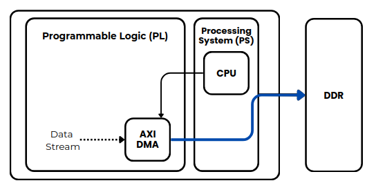
The following figure shows how data can be sent from a custom IP to the DDR memory through the Processing System (PS). In this case, an AXI DMA is required to act as an intermediary between the AXI4-Stream interface and the High-Performance AXI port of the PS. In this article, we created a Python driver that configures the AXI DMA to perform the desired transaction.
However, when we want to do something similar without a Processing System (PS), things are quite different. First of all, in this case we don’t have a PS with a Memory Management Unit (MMU) to manage the DDR. Instead, we need to include and configure a Memory Interface Generator (MIG) in order to send and receive data from the DDR.
What makes this approach a bit more complex is that the MIG uses an AXI4 Memory-Mapped (AXI4-MM) interface. This means we must provide both the address and the data for every word we want to store in external memory. In a regular AXI4-Stream transaction, we simply configure the destination address—the address of the first data word—and the remaining data is written to consecutive addresses. This is exactly what we did when configuring the AXI DMA.
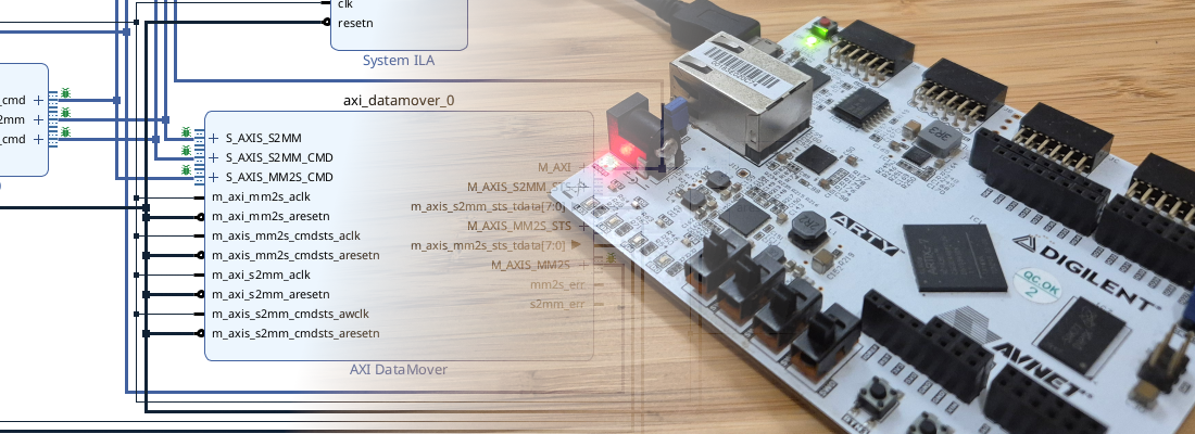
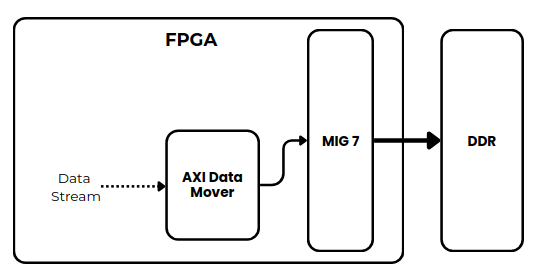
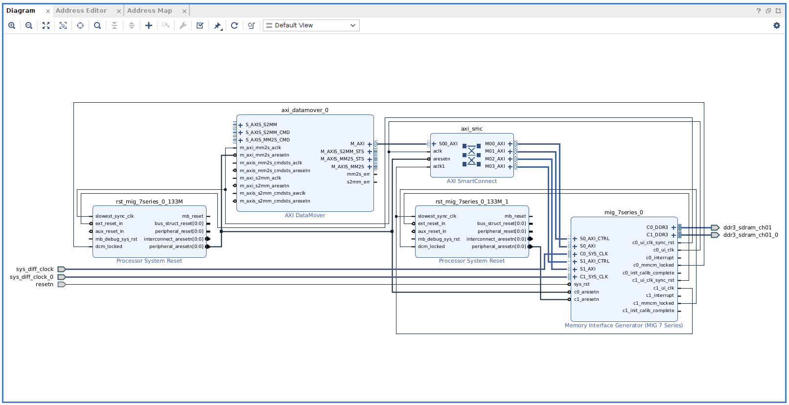
To enable this type of transaction without a PS, we have a couple of options. The first is to create a custom driver that increments the address for each data word. The second—and simpler—option is to let AMD handle it by using the AXI Data Mover IP.
This IP acts as a bridge between the AXI4-Stream interface and the AXI4 Memory-Mapped interface. The following figure shows the resulting diagram.
Devices that can bennefit of this kind of applications are FPGA-based hardware accelerators. These devices receive data from the host computer, process it, and then return the results. For example, if we are using the Kintex7 accelerator, the followinig diagram can be used for this application.
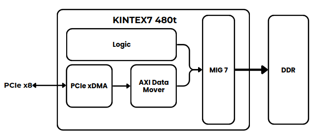
In the diagram, we can see how the DDR memory can be filled from the PCIe interface through the PCIe xDMA IP, where the DMA is configured to implement an AXI4-Stream interface. Then, this stream of data is sent to the DDR via the AXI Data Mover.
On the other side, in the Programmable Logic (PL), a custom IP can read data from the DDR to execute the desired algorithm.
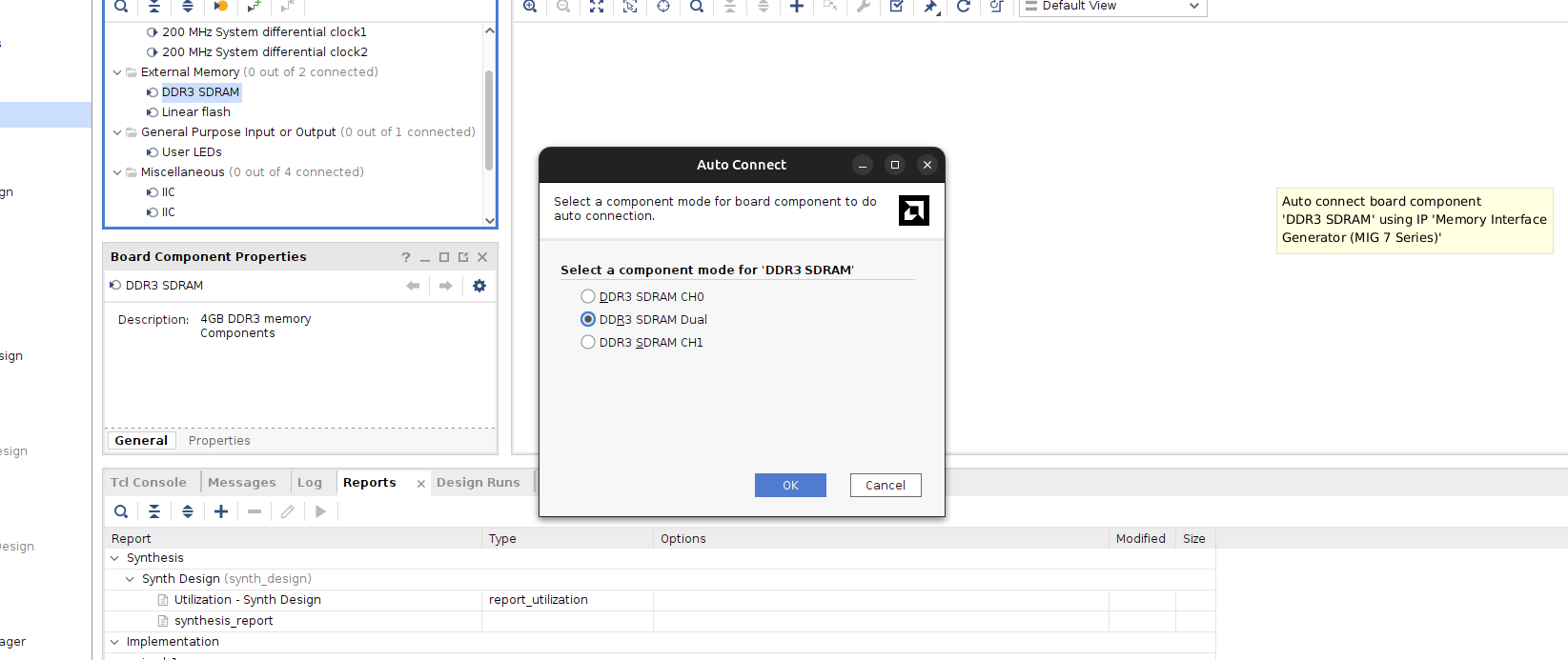
To bring this design to the YPCB-00388-1P1 board, we first need to create a project in Vivado, then create a block design, and add the MIG by dragging the DDR3 component of the board into the canvas. Vivado will prompt us to choose which DDR memory configuration to use. We can select a single channel, or both channels in a dual configuration.
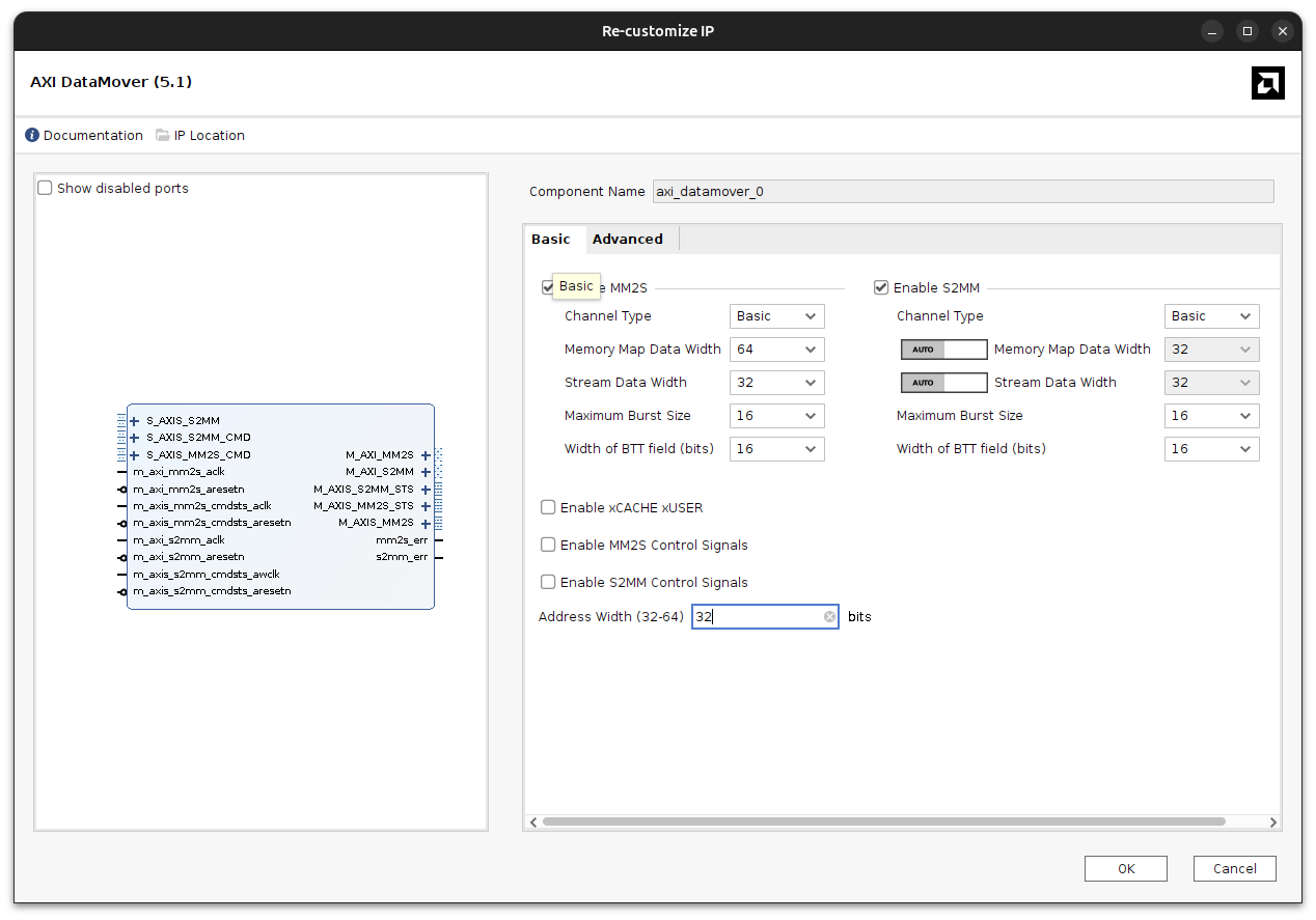
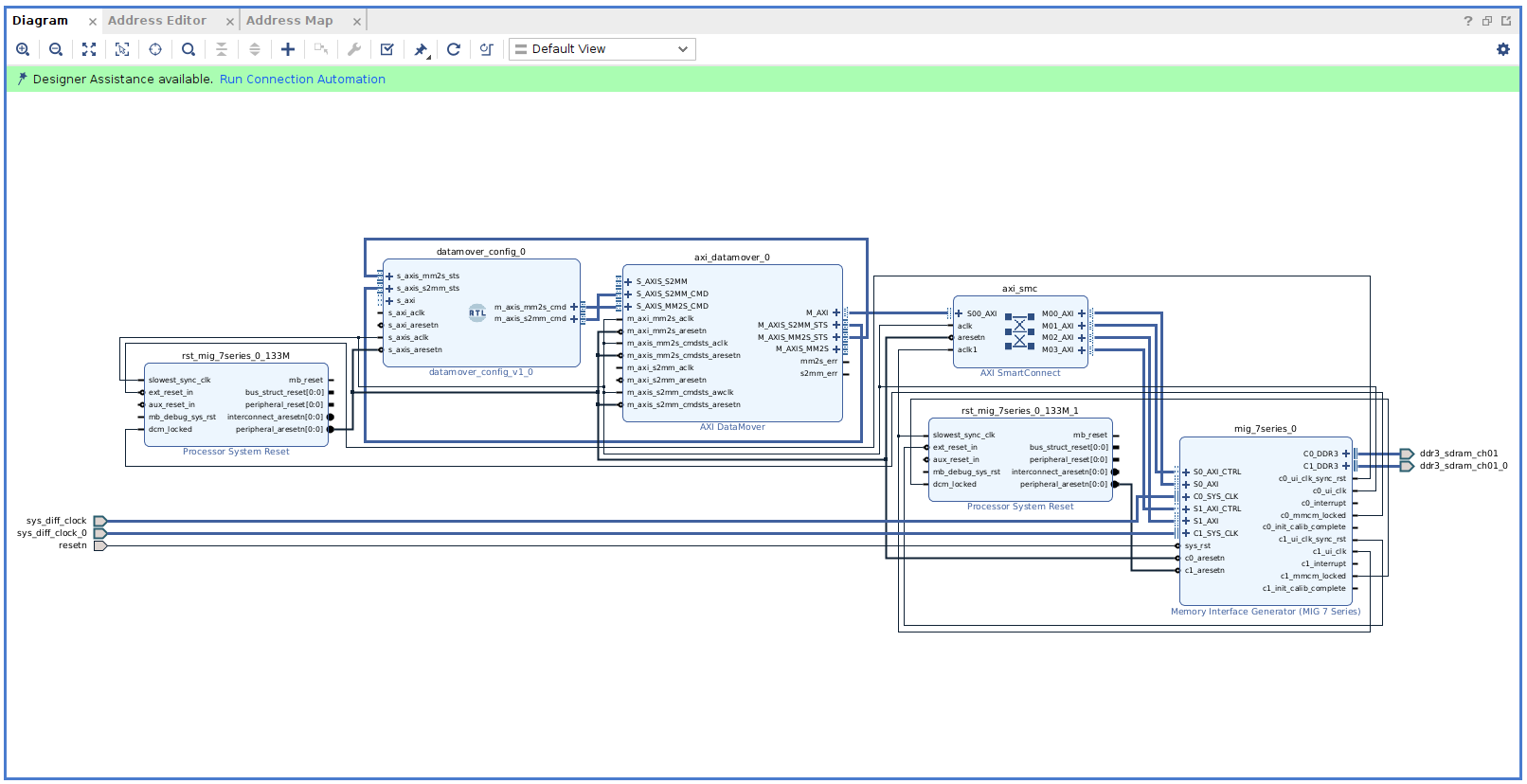
Then, we can add the AXI Data Mover, and connect it to the MIG. The configuration of the AXI Data Mover is very similar to the configuration ox the AXI DMA. It allows to configure widths and the maximum burst size.
To connect the IP to the MIG, Vivado will display the Run Connection Automation pop-up. We can open it to automatically generate the necessary connections.
It’s important to note that when using a MIG, it generates its own clock based on the DDR memory speed, and this clock must be used to perform DDR transactions.
The AXI Data Mover uses four different clocks: one for the AXI4-MM S2MM channel, another for the AXI4-MM MM2S channel, and two more for the AXI4-Stream command interfaces. The AXI4-Stream interfaces (MM2S and S2MM) must be clocked using the DDR clock, which in this case is 133 MHz.
This is crucial, as these interfaces cannot operate with an arbitrary clock source.
In the Address Editor, we can see that the 4 GB of DDR memory have been correctly allocated.

At this point, we have the AXI Data Mover connected. To configure the transaction size, as well as the source and destination addresses, we need to use the command interface channels: S_AXIS_S2MM_CMD and S_AXIS_MM2S_CMD.
These channels are 72 bits wide, but according to the diagram in the AXI Data Mover User Guide, only the lower 40 bits are actually used.
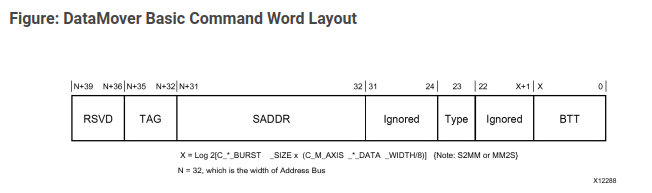
In the command register, we can find several fields:
SADDRConfigures the start address for the source or destination.BTTSpecifies the number of bytes to transfer in the transaction.TYPEDefines the type of transaction. This field allows us to specify whether the address should increment with each transfer or remain fixed, writing repeatedly to the same address.
To configure the command register, I created an RTL module that sets all the fields according to the configuration received through an AXI4-Lite interface. (You can use the AXI4 Slave generator for this purporse).
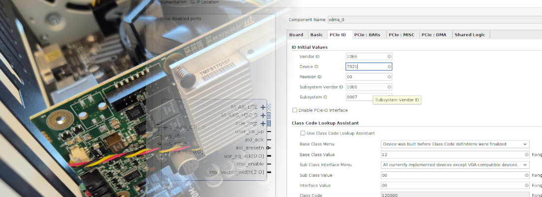
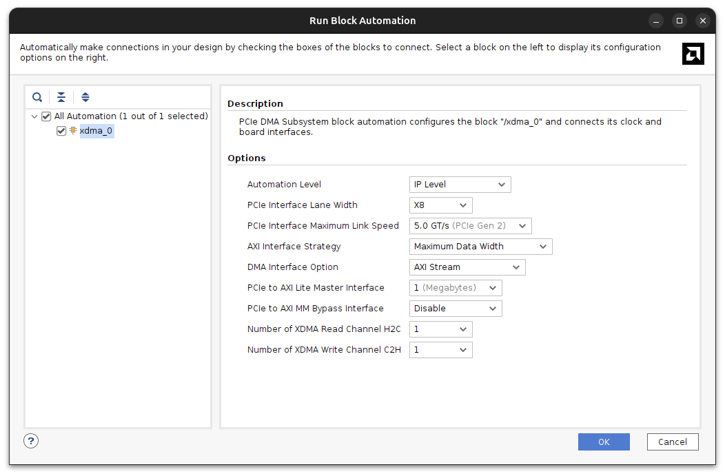
Finally, we need to add the DMA/Bridge Subsystem for PCI Express. In its configuration menu, we must enable the PCIe to AXI-Lite Master Interface in order to have an AXI4-Lite Master accessible from the host PC. Additionally, we need to switch the DMA Interface option to AXI Stream.
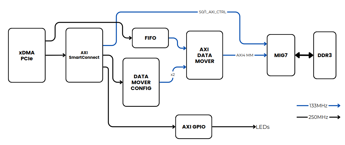
Now, we need to discuss the clock domains. The PCIe IP operates with a 250 MHz clock derived from the PCIe interface, which is not compatible with the 133 MHz clock generated by the MIG. In the following figure, you can see a simplified diagram of the design, including the required clock frequencies for each module.
Note that we need to insert a FIFO between the AXI4-Stream interface of the PCIe xDMA and the AXI Data Mover to safely handle the clock domain crossing. Additionally, the AXI SmartConnect must operate with two different clocks: one for the general AXI interconnect logic, and another for the AXI4 control interface connected to the MIG, which must use the MIG-generated clock.
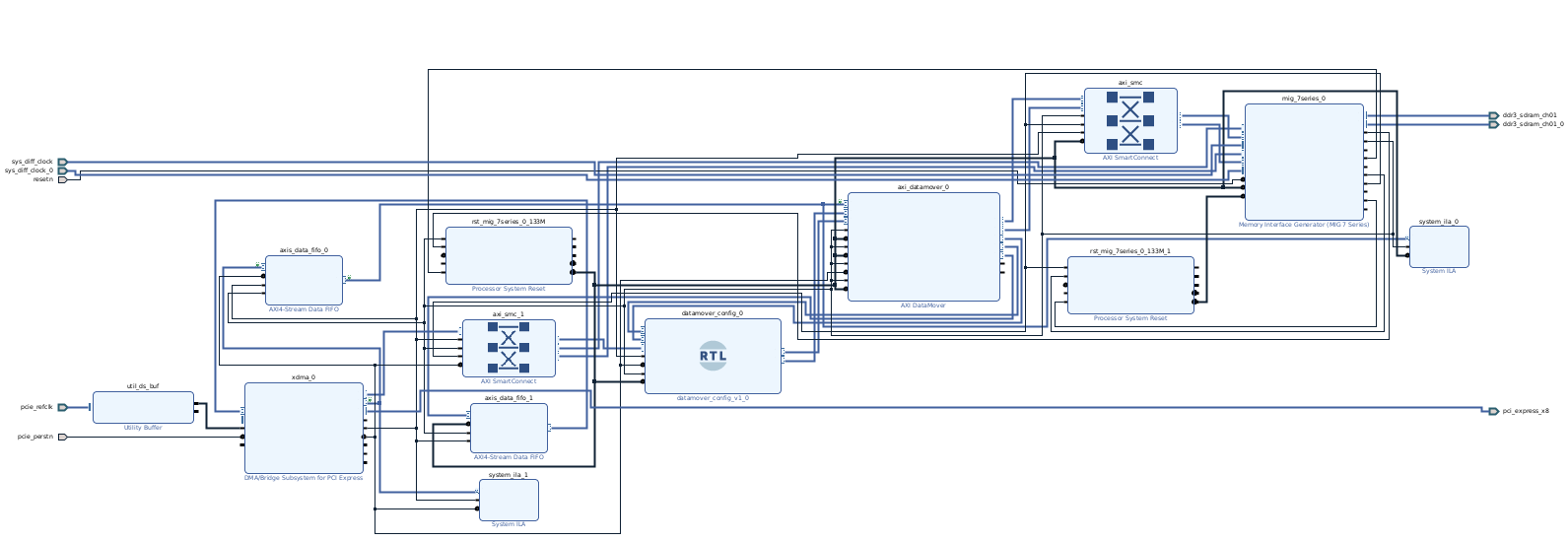
Finally, the complete block design is the next.
In a future article, we will discuss the software side of this project, which is not as complex as the hardware side.
That FPGAs are powerful when used as hardware accelerators is something you likely already know—especially if you’re a regular reader of this blog. But the combination of PCIe + FPGA + DDR is even more powerful.
The approach discussed in this article is well known when it comes to transferring data between computers. However, doing it between a host computer and an FPGA allows us to leverage all the advantages of FPGA acceleration within the data path.