Designing an FPGA board.

Few month ago, I decided to design my own FPGA development board. The main reason for that was simply learn to do it, because I have design a lot o boards for peripherals, PMODs, or other projects, but never one based on FPGA, and for me, route a BGA was a big challenge.
When someone start a board project, the first that have to do is to select the components, and this may seem basic, but if the purpose of your design is assembly the board, is important to select components be easy to buy for you, or for your manufacturer. Following this guideline, first component that I have selected is the FPGA. I need an cheap FPGA, because I know that I will need some iterations to complete the board, and I don’t want spend a lot of money with each iteration. Also, I want to use the FPGA for implement some digital signal processing algorithms, so I need an FPGA with many DSP slices. Last, my idea is not use an external RAM, so all data have to be stored on internal RAM blocks. With all of these requirements, I need to select a Part number, and also, a Package. In my case, I have select an Spartan 7, in particular the part number xc7s15, with the package FTGB192. The reasons to select this piece are the price, we can found this part on Mouser for 15,88€, it has 20 DSP slices, that are a good start for several digital signal processing algorithm. Regarding BRAM, that is not the high point of this piece, but, here come the reason for select FTGB196. Besides it uses a pitch of 1mm, enough to manufacture a cheap board, this package is the most used on Spartan 7 series, so with the same PCB, I can assembly from xc7s6 to xc7s50. Regarding the speed grade and temperature, I’ve select the cheapest, -1, and commercial grade.

Once we have our FPGA, the next is the components to make that FPGA works correctly. First, we have to supply the FPGA with the correct levels. For chek what are the correct levels, and their tolerances, we need to check the datasheet, in this case, the Spartan-7 FPGAs Data Sheet (DS189), and check the correct voltage levels for the different supplies.

As we can see, for this FPGA we need 3 different sources, 1V (Vccint, Vccbram), 1V8 (Vccaux), and 3V3 (Vcco). Also, we have to take in mind the external components what will be supplied by the corresponding power supply, for example, in my case, 3V3 power supply, will also supply external peripherals, so we have to overrate this power supply. Regarding the topology, for make a simple design we can use LDO, and is the option that I have selected for the first revision, but for a final revision, and taking care about the efficiency and temperature, the best choice are the switching converters.
Regarding the clock, the best choice is to select an integrated oscilator. In my case I have select a 30MHz, LVTTL oscillator. Regarding the connection to the FPGA, we will take care that the pin where we connect the oscillator, has to be a pin connected to the internal clock lanes. In general, on Xilinx 7 series, these pins are named as MRCC (Multi Region Clock Capable). In case of using an integrated oscillator, we only have the positive pin of the oscillator, so the connection must be at MRCC_P pin.
Xilinx’s FPGA are base on RAM, so we will need a non-volatile storage to store our design. IN general, for that purpose FLASH memories are used. IN this case I have used a FLASH memory with 64Mb, that is enough for the size of the FPGA.
The next that we will think are the peripherals that we want to connect to the FPGA. If we want to design a general use board, the best choice is select the the less peripherals as we can, and include on our design some external connectors. In my case, I have select 2 different types of connectors, that are corresponding with the 2 most used standards, PMOD from Digilent, and MikroBUS from Mikroe. Using these standars, our FPGA board will have access to a large number of peripherals. Also, it is good to include on the board some leds for fast testing and some push buttons.

Once we will select all components of our design, the next is the schematic design, and routing. In my case, and what I will write now is only the way I work, I draw the schematic of all fixed lines on my board, that is, lines that only can be routed to 1 pin, except supplies. When I have this lines on my schematic, I start the PCB by the placement, and then I route this lines. Wten all this lines are routed, I start to work with non fixed lines on schematic and PCB at the same time. This make easy for me select the pins by checking the result on the PCB on real time. Once all this non-fixed lines are routed, the last is route the supplies.
This design, where the FPGA has 196 pins with 1mm of pitch, and assuming that not all the pins will be used, I have select a 4 layers PCB. Using a 4 layer PCBs we will have a large amount of possibilities of routing, with a low fabrication cost.

Now, when I have finished the design, and check that there are no errors, is proceed to the fabrication. In general, when I design a PCB, I use a manufacturer like PCBWay to PCB fabrication, and I make the assembly. This way is very economic, as we can have a professional PCB for 5$.
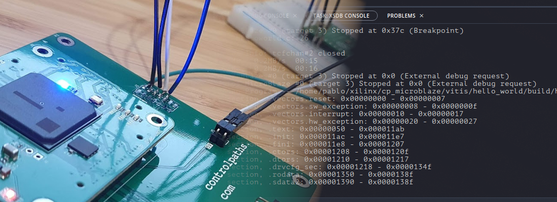
In this case, where the board has BGA components, and other very small components, I prefered a professional assembly, so this time I have used the PCB Assembly service of PCBWay.
Once the order has complete, they contact me in some times to ask me about the non-route lanes, the position of the components, and even they send me the X-ray images for ensure that all is ok, and this contact is very appreciated for me, becaus it allow me to detect some mistake before the board is completed.
Once the order has complete, they contact me in some times to ask me about the non-route lanes, the position of the components, and even they send me the X-ray images for ensure that all is ok, and this contact is very appreciated for me, becaus it allow me to detect some mistake before the board is completed.


Next is to fix some mistakes that I made on design, change the LDO by switching supplies, and test all for the next revision, and I hope the final revision. Thanks for read!