Using MATLAB and FPGA-in-the-Loop to design a filter (Part 2)

In the last post, we had designed a filter with filter designer tool from MATLAB. After verifying the filter on MATLAB and Simulink, we have to generate the HDL and verify the implementation using FPGA-in-the-Loop, and later, verify the filter on the real design.
To generate the HDL, first, we have to make a change in the Simulink model. When the filter model is inserted on Simulink model, MATLAB add a subsystem that contains a Biquad block, that is corresponding to the filter, and a Convert block to convert from a double signal to a quantified signal. Since we are going to generate the HDL of the entire subsystem, we need to delete the Convert module of the subsystem and copy it on the main model.

The main model will look like the next.

Once the model has been modified, on the filter subsystem we have to configure the HDL implementation of the filter. Inside the filter subsystem, on Biquad block, right-click and HDL Code > HDL Block properties. And a window like this will be opened. On this window, we can configure the pipeline registers and the architecture in terms of multipliers used. We can choose 3 different architectures:
- Fully Parallel architecture, where each multiplication of the filter will use one DSP Slice of the FPGA, and the output data frequency can be the same as the clock frequency.

-
Fully serial architecture, where only 1 DSP Slice will be used. This architecture is the best in terms of DSP used, but all the logic added to manage the DSP Slice pipeline can increase the FPGA occupied slices. Also, the output frequency will be reduced up to clk/mulltiplications. The reason is to compute one sample, the design has to perform ‘x’ multiplications using only one DSP Slice, so all the multiplications are queued. With this configuration appears a new term named folding and folding factor. Folding is basically adding a multiplexor n to 1 on the input of the multiply-accumulator block, where n are the multiplications that filter has to perform. Using this configuration on MATLAB, the folding factor is maximum and the throughput is low.
-
Partially serial architecture is in the middle. With this configuration we can select the number of DSP Slices we want to use, or the folding factor. The throughput of the system will vary according this configuration.

To select this parameter, we have to think on our design. In this case, input data has a sample rate of 10MHz, and the clock of the design will be 100MHz, so we have 10 cycles between samples, that means we only can perform 10 multiplications. To compute an 8th order filter, we need 16 multiplications, so the Fully serial configuration can be discarded. To see the difference between the other 2 architectures we will test both. First, we will test Fully Parallel architecture. Regarding pipeline registers, I don’t expect have Timing problems, so we don’t add them.
Now on the main model, right click on the filter subsystem HDL Code > HDL Coder Properties. On this window we can select the target HDL language, the device we will use. On global settings tab we can select the reset type. In my case I have select a synchronous reset. Last, on Report tab, we will select all the reports to check the implementation.

When all the configurations are done, right click on the filter subsystem and Generate HDL for Subsystem. This step may cause errors if your Simulink model use blocks To workspace and From workspace, to void these errors, you can copy the filter subsystem and the input Convert block to a new Simulink model and it works without errors.
Once the HDL is generated, a window will be opened with the report. If we open the High-Level Resource Report, we can see that design uses 16 multipliers.

If we repeat all the process, but using only 3 multipliers, we can see how the number of multiplexers grow.

On the .v file, we can see the folding factor used.

At this point we have the HDL of the filter, and next we are going to perform a simulation, but the filter will be executed on the FPGA. To do that we will use FPGA-in-the-Loop. To start this simulation, we have to open filWizard tool.

First we need to create the board definition to allow us connect the board through FIL. To do that, on the opened window, we have to click on Launch Board Manager. Then we will search for ZedBoard since is based on the same FPGA than Eclypse Z7. Then click on Clone…

One we have configured the name and the location of the xml file of the board, a configuration windows will be opened. Since our board is cloned from ZedBoard, all the fields of the new window are filled, but we need to change the fields that are related directly with the board, like clock and reset. In the case of Eclypse Z7, clock source connected to PL, is generated but the ethernet phy, and has a frequency of 125MHz, and is connected to pin D18. Eclypse Z7 has no a dedicate reset button, but this is not a problem because it is no needed to create a FIL board.

Once the board is defined, click on OK, and the board will be selectable on the list. The next is Validate the connection to the board. Is we click on Validate, a new window will be opened, now we have to configure the connection as JTAG, and we have to check the box to include the board on the test. When we click on Run Selected Test(s), a popup will advise us that the test can spend up to 30 minutes. We have to click on Yes, and Vivado will be opened on the MATLAB command window and it start to synthesize and implement the FIL demo design.

If the test failed, you can check if MATLAB command window will ask you about Digilent Adept.

To fix that we have to download the Digilent Adept Runtime from Digilent’s webpage. Once the runtime is installed, the validation will be Passed.

Now, on the initial Fil Wizard Board, we can select our new EclypseZ7 board, the connection to the board, in this case only JTAG will be available, and the speed of the main clock of the FIL simulation.

By clicking on Next, the next window ask us about the HDL files. In this case we will add the HDL with the fully parallel implementation, and we will indicate that the filter is the top level.

MATLAB will parse our file or files looking for the ports, clock signals and reset signal, and it show us the results.

On the next window, we have to configure the format of the output data. This step is needed to see the output results on Simulink correctly. In our case, output data has a width of 18 bits, and the fractional part is 13. Notice that the sign by default is unsigned, and for the output signal that is wrong, correct configuration is signed.

Finally, MATLAB show us a summary of the project, and clicking over Build, Vivado will be opened on tcl mode and the run starts.

When Vivado finish the synthesis, a Simulink model will be opened with the FIL block.
Now, we can connect our Eclypse Z7 board, open the FIL model and clicking on Load, the model will be load on the FPGA.

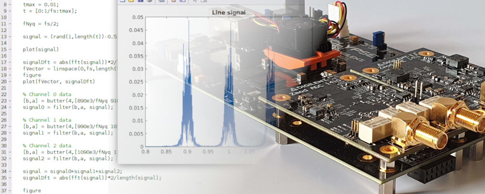
On model I have used to perform this simulation, I have added 3 sine signals that represents the 3 bands in our transmission line, frequencies of this signals are 900kHz, 1MHz and 1.1MHz. To verify the output, I have added an Spectrum analyzer.

When the simulation finish, the output on the Spectrum will looks like this. We can see 3 peaks on 900kHz, 1Mhz and 1.1MHz of the input signal, and the output only contains the 1MHz signal.

To see the entire band-pass behavior, we can connect at the input a noise source (Band limited white noise), and check the limits of the band-pass. In this case, the gain difference on the band-pass is 3dBm.

Once we have checked the RTL implementation of the filter, we can add the filter to our design. On Vivado, I have created this block design that contains the AXI Stream IP to manage the ZMOD ADC, a Clocking wizard to get the 100MHz clock, and a clock enable generator to generate the correct clock enable to the filter. Also, to verify the behavior, I have added an ILA.

To test the entire design, I will use a Rigol Arbitrary waveform generator configured to generate a white noise signal. Data acquired by ADC, that is the same as the filter input, and the filter output will be saved by ILA. Then, ILA data will be written on .csv file with the next TCL instruction.
write_hw_ila_data -csv_file /home/pablo/matlab/filterdesigner_1/ila_data.csv [current_hw_ila_data]}
Now, performing the DFT to the input and output data, we can see that the filter output is always around 1MHz, and bands on 900kHz and 1.1MHz still clean.

On last 2 post I have proposed you a workflow from the design step to test the filter on the real application. For me, it is important check that the response of the filter is the same after each step because in case of an error, will be easiest find the wrong step and fix it. MATLAB allow to design and verify all the steps without leave the program, and it is very interesting. The application I have develop is only an example for this workflow, and I hope it helps you to design and test your filter.
All code scripts are available on Github and FileExchange.